-
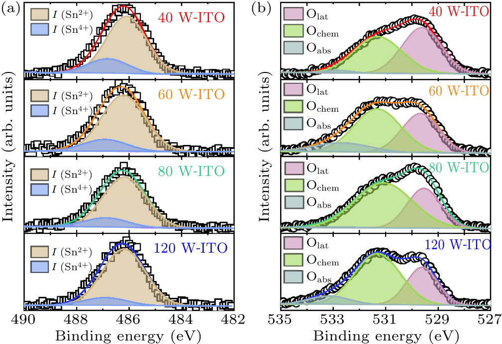
Figure 1. Fitting analysis of XPS spectra of Sn 3d5/2 and O 1s in the ITO films prepared under different sputtering powers. (a) The Sn 3d5/2 signals are deconvoluted into two Gaussian components, corresponding to the presence of Sn2+ and Sn4+, respectively. The measured data and fitting curves are shown as open squares and solid curves, respectively. (b) The O 1s spectra are resolved into three Gaussian components, attributed to lattice oxygen (Olat), chemisorbed oxygen (Ochem), and adventitious oxygen species (Oabs). The measured data and fitting curves are shown as open circles and solid curves, respectively.
-
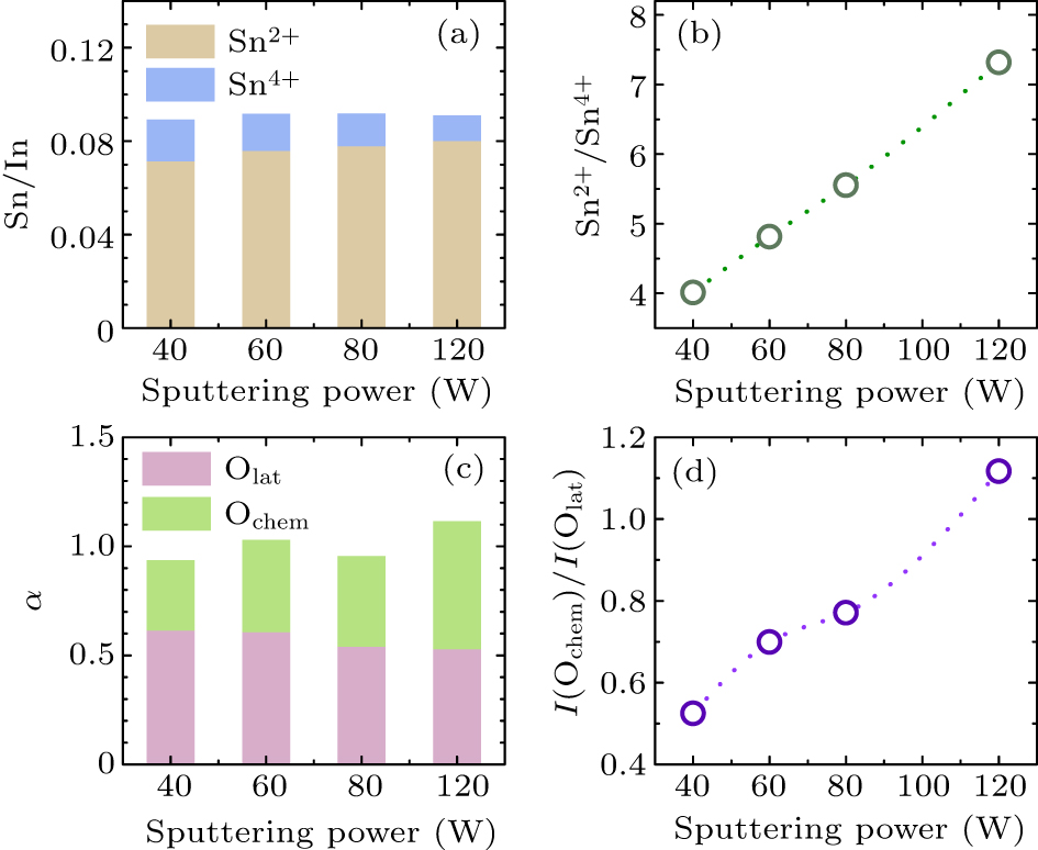
Figure 2. The relationship between the chemical composition of ITO films and the sputtering power. (a) The Sn/In atomic ratio in ITO films remains nearly constant as the sputtering power increases from 40 W to 120 W. (b) ITO films deposited at higher sputtering powers possess a higher atomic ratio of Sn2+/Sn4+. (c) The overall oxygen content within ITO films reaches near-stoichiometric levels via combined effects of lattice oxygen and chemisorbed oxygen species. (d) The relative content of chemisorbed oxygen increases with rising sputtering power, indicating a corresponding increase in oxygen vacancy content.
-
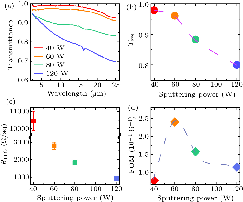
Figure 3. The infrared optoelectronic performance of ITO films with sputtering powers of 40 W, 60 W, 80 W, and 120 W. (a) The infrared transmittance progressively decreases with increasing oxygen vacancy content, which is modulated by sputtering power. (b) The average infrared transmittance (Tave) decreases with increasing oxygen vacancy content. (c) The sheet resistance of ITO films monotonically decreases with increasing sputtering power, which indicates that the enhanced oxygen vacancy content improves the electrical conductivity. (d) The FOM value reaches the maximum in the 60 W-ITO sample, suggesting that a moderate oxygen vacancy content benefits the infrared optoelectronic performance.
-
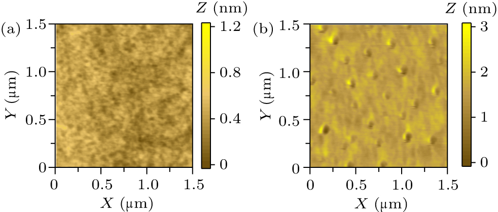
Figure 4. (a) Surface morphology of the bare ITO bottom layer in Cu/40 W-ITO samples (without Cu capping layer). The ITO bottom layer exhibits a relatively smooth surface. (b) Surface morphology of the Cu-20 s/40 W-ITO sample with a Cu capping layer, indicating an island-like structure of the ultra-thin Cu layer through the presence of semi-ellipsoidal hillocks on the film surface.
-
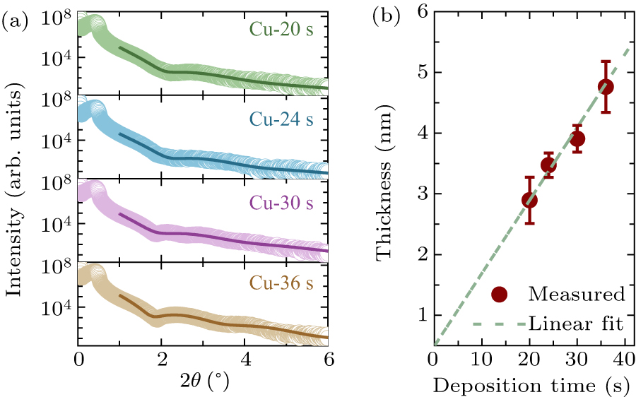
Figure 5. The thickness characterization of ultra-thin Cu films deposited on Si wafers. (a) The XRR spectra of ultra-thin Cu films with deposition times 20 s, 24 s, 30 s, and 36 s. The measured data and fitting curves are represented by open circles and solid lines, respectively. (b) The quantitative relationship between the film thickness, equal to the sum of the thicknesses of the interfacial layer and the bulk-like layer, and deposition time. The linear fitting process shows that the film thickness is nearly proportional to the deposition time. The thicknesses of Cu-20 s, Cu-24 s, Cu-30 s, and Cu-36 s films are estimated to be 2.893 nm, 3.472 nm, 3.906 nm, and 4.716 nm, respectively.
-
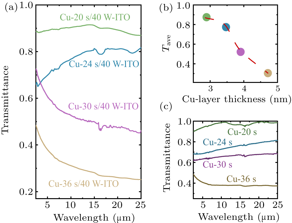
Figure 6. (a) Infrared transmittance spectra of Cu/40 W-ITO with various Cu capping layer thicknesses. (b) The relationship between the average infrared transmittance of Cu/40 W-ITO films and the Cu capping layer thickness. (c) Infrared transmittance spectra of ultra-thin Cu layers deposited on KBr substrates.
-
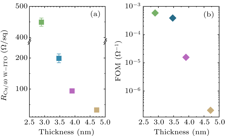
Figure 7. (a) Sheet resistance values of Cu/40 W-ITO films with different Cu capping layer thicknesses. (b) The relationship between FOM values of Cu/40 W-ITO films and the Cu capping layer thickness.
-
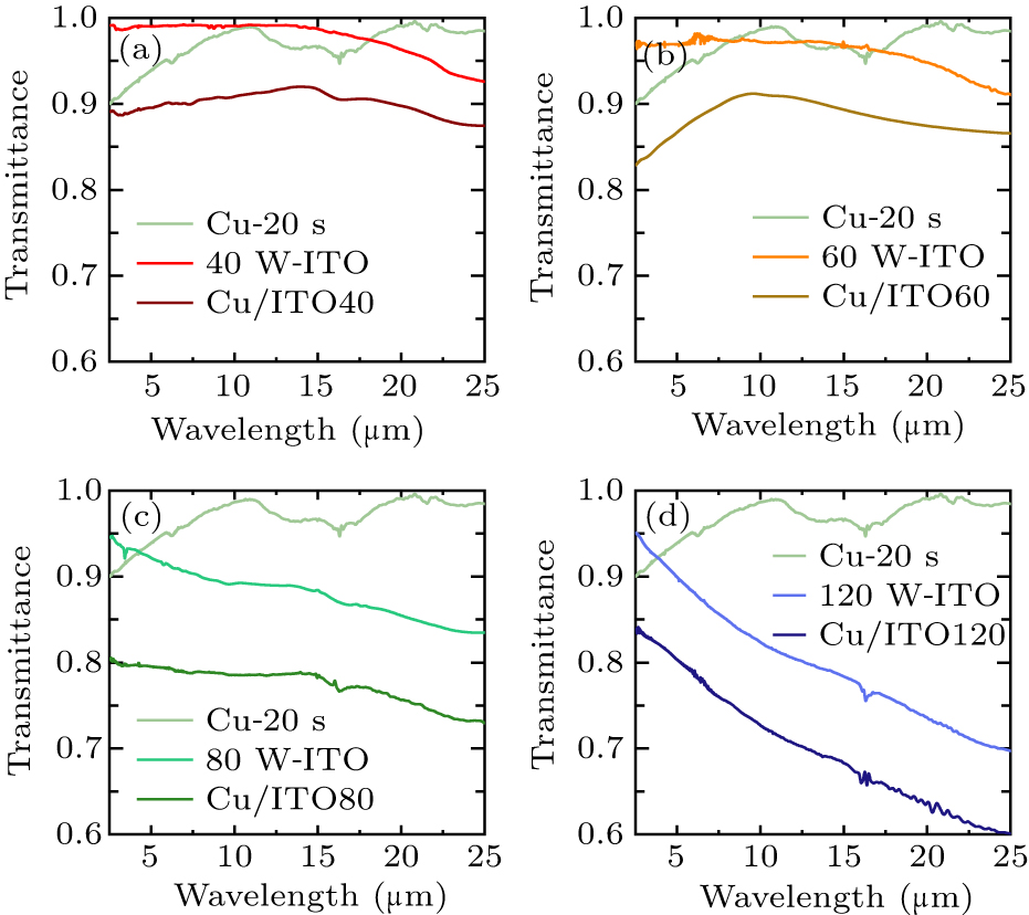
Figure 8. The effect of the Cu capping layer on the infrared transmittance spectra of ITO films with various oxygen vacancy contents. The introduction of a Cu capping layer leads to a slight decrease in the optical transmittance of the Cu/ITO bilayered film compared to that of pristine ITO film.
-
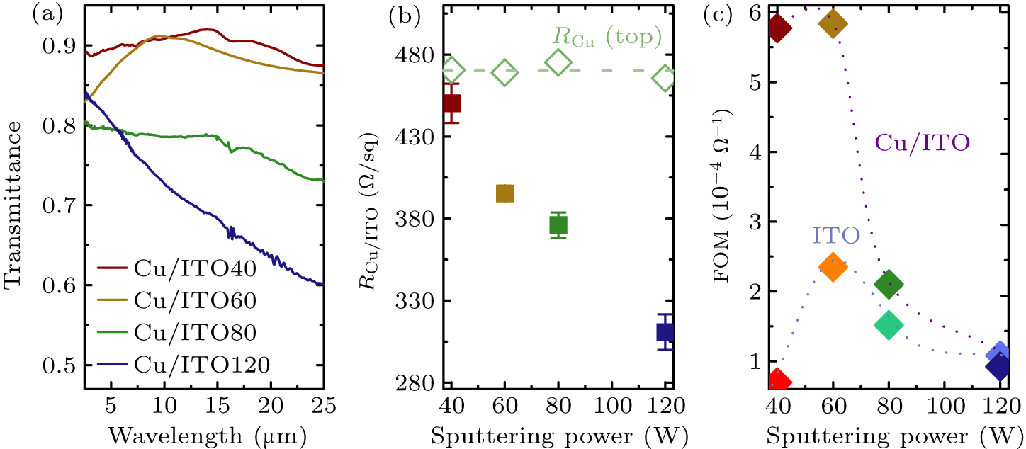
Figure 9. The relationship between the infrared optoelectronic performance of Cu (3 nm)/ITO bilayered films and the oxygen vacancy content within the ITO bottom layer. The oxygen vacancy content within the ITO layer exhibits a positive correlation with sputtering power. (a) Infrared transmittance spectra of Cu (3 nm)/ITO bilayered films with varying oxygen vacancy content in the ITO layer. (b) The relationship between sheet resistance of Cu (3 nm)/ITO films and oxygen vacancy content within the ITO layer. The sheet resistances of the Cu capping layers, calculated based on a parallel conductive network, are also shown as a reference. (c) The relationship between the FOM values of Cu (3 nm)/ITO films and the oxygen vacancy content, including a comparison with pristine ITO films.
Figure
9 ,Table
1 个