-
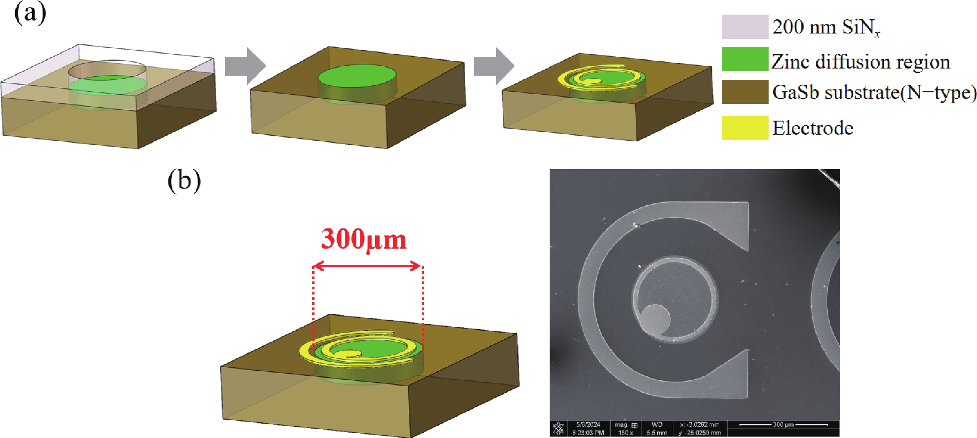
Figure Fig. 1. (Color online) (a) The process of planar structure photodiode fabrication through diffusion and the final device structure. (b) SEM diagram of the fabricated devices.
-
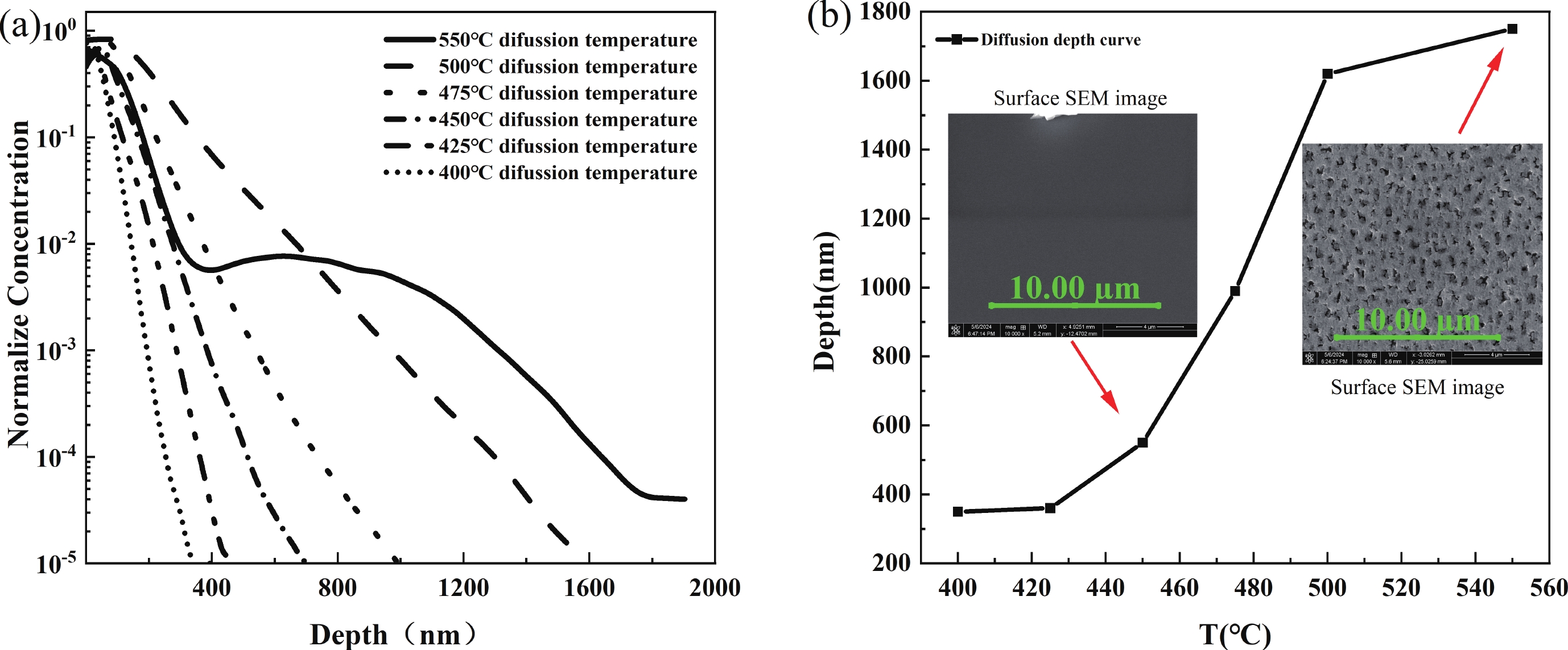
Figure Fig. 2. (Color online) (a) SIMS test results. (b) The relationship between diffusion depth and diffusion temperature.
-
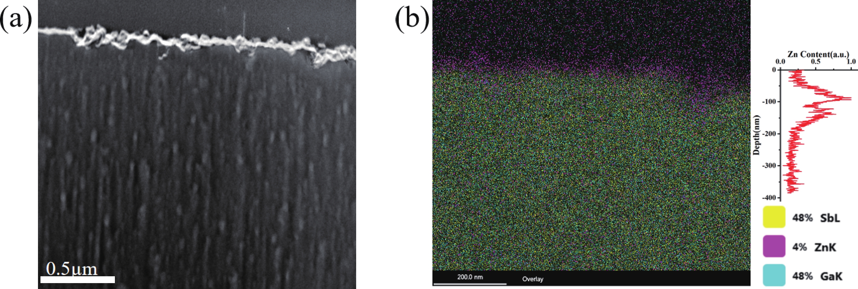
Figure Fig. 3. (Color online) (a) The cross-section TEM image and (b) mapping energy spectrum of fabricated planar PN junction detector.
-
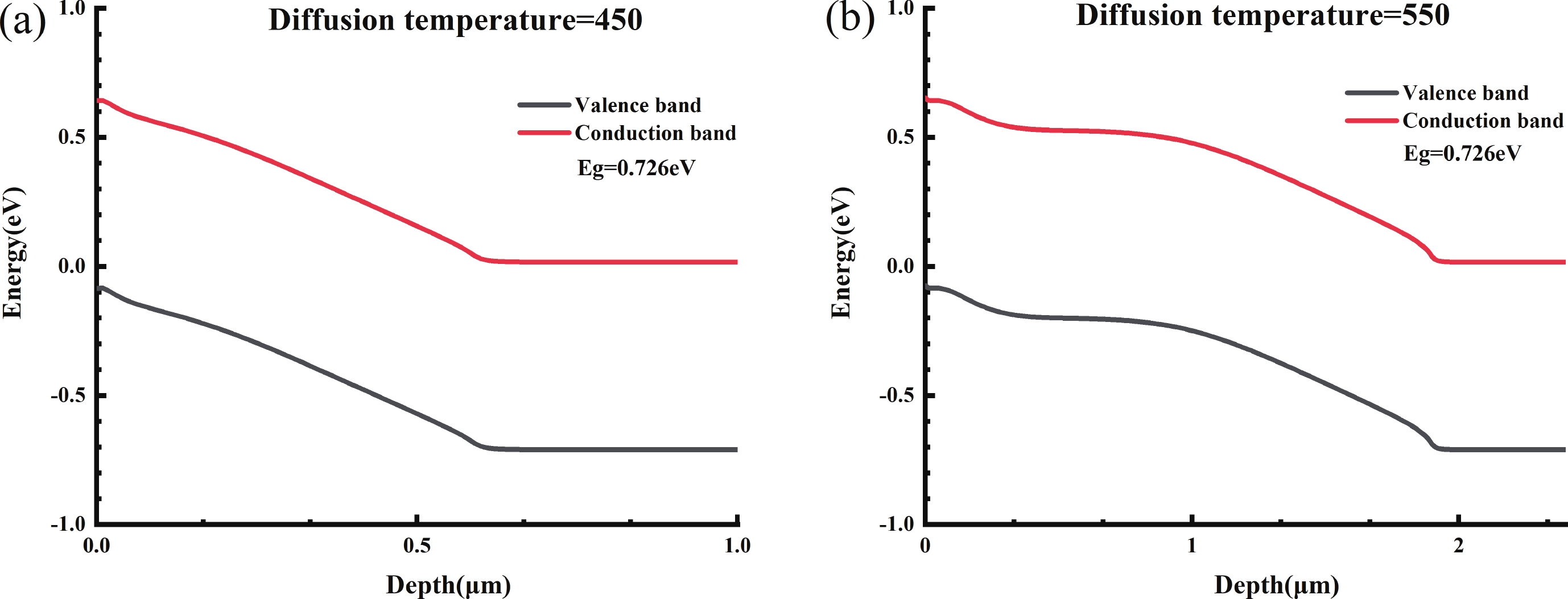
Figure Fig. 4. (Color online) Simulation result of band structure based on SIMS data with a diffusion temperature of (a) 450 °C and (b) 550 °C.
-
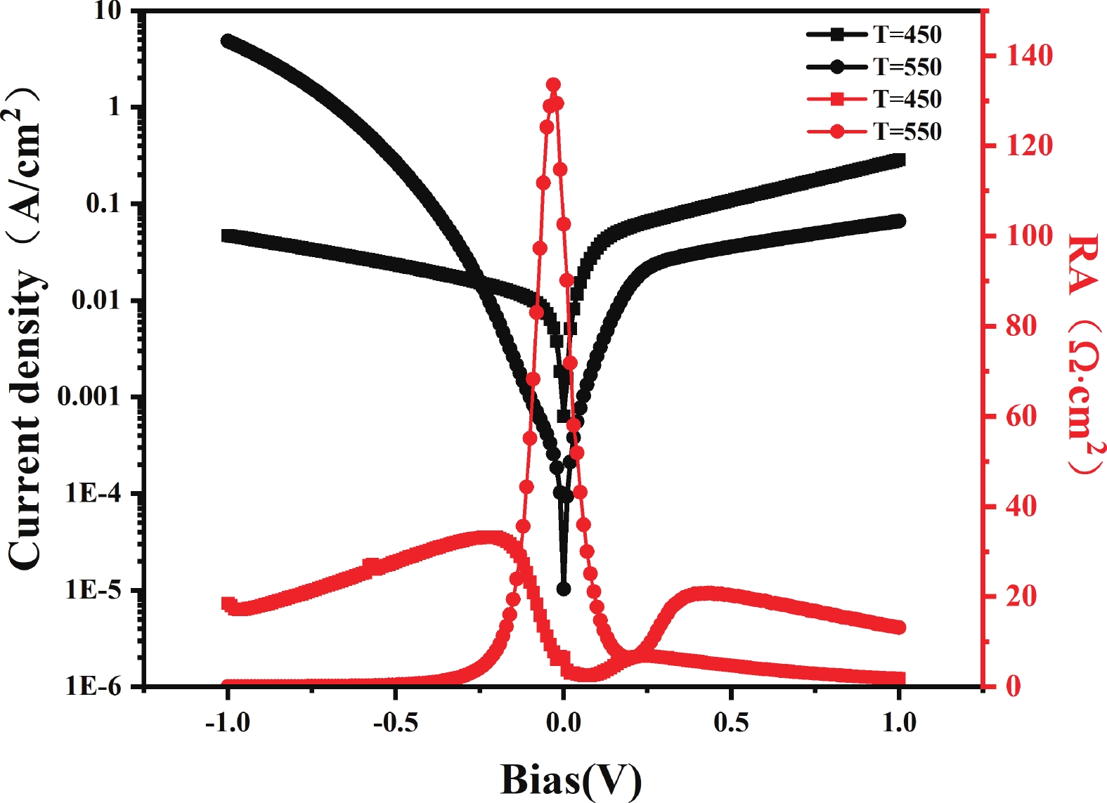
Figure Fig. 5. (Color online) The relationship between dark current density and bias at different temperatures for devices with diffusion temperatures of 450 and 550 °C.
-
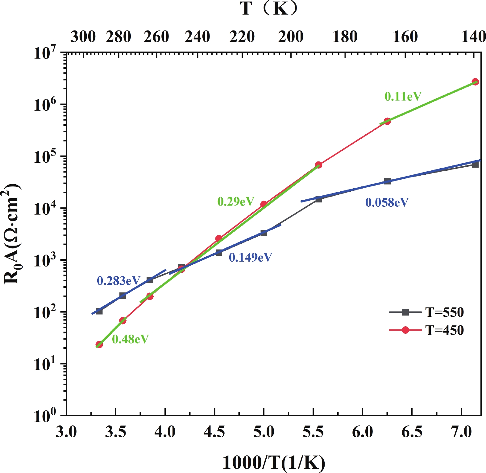
Figure Fig. 6. (Color online) The dark current mechanism of samples diffused at 450 and 550 °C.
-
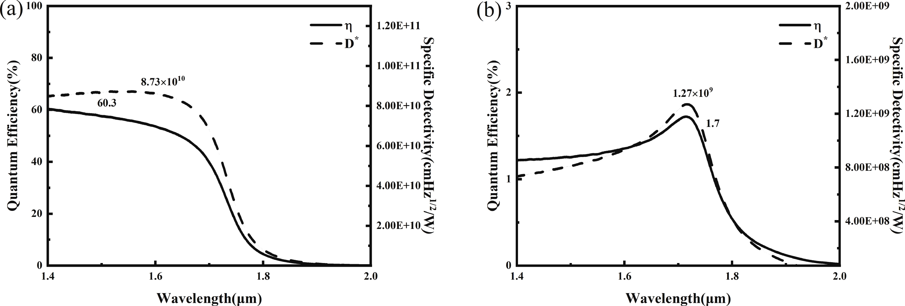
Figure Fig. 7. Performance curve and wavelength of the photodiode with a diffusion temperature of (a) 550 °C and (b) 450 °C.
-
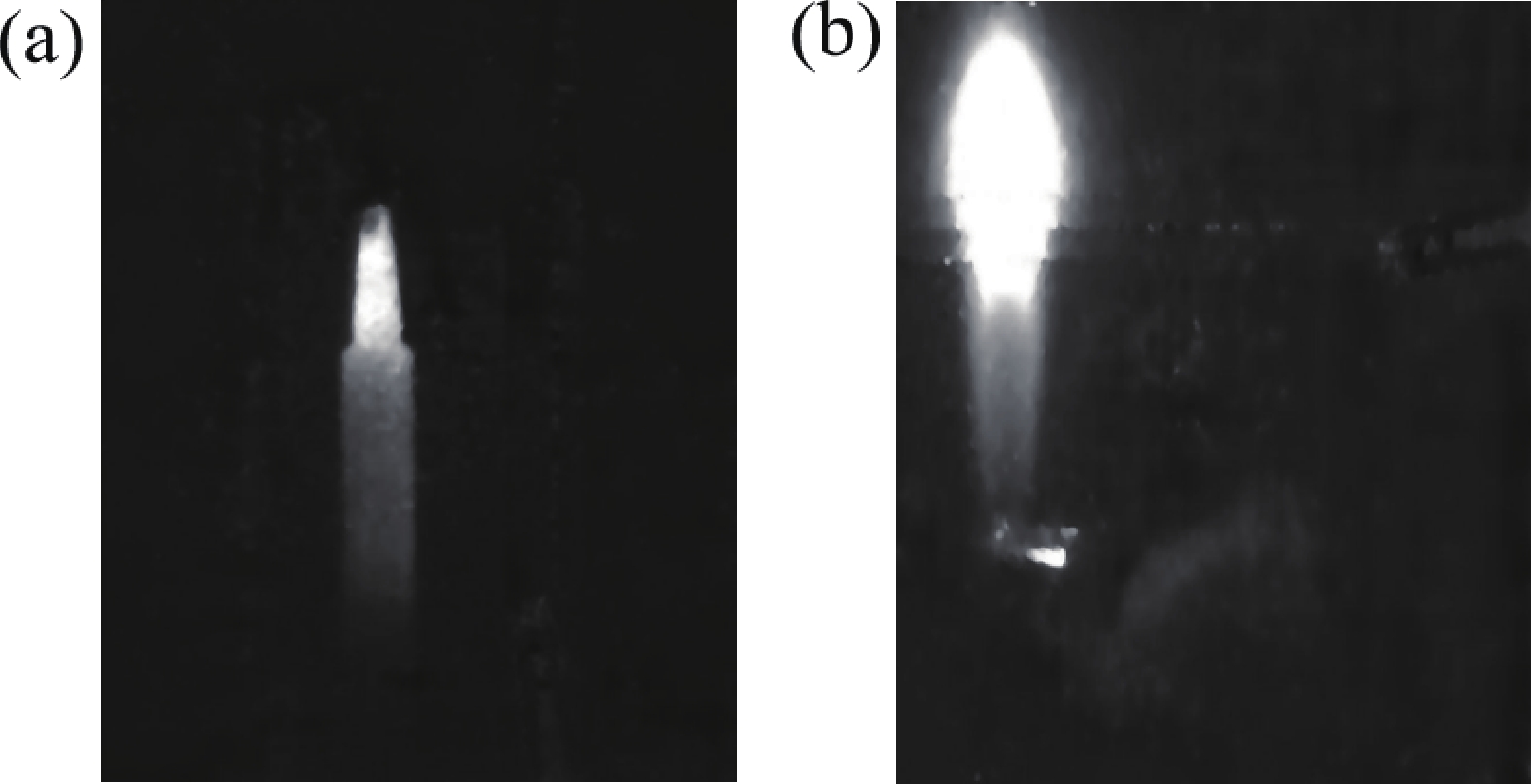
Figure Fig. 8. Infrared radiation imaging of (a) electric soldering iron and (b) lighter flame.
Figure
8 ,Table
1 个