-
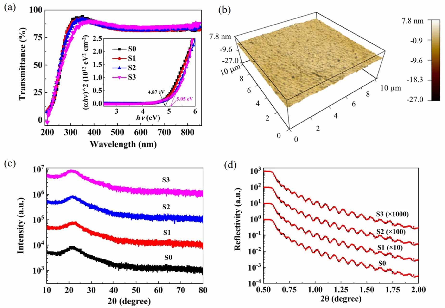
Figure 1. (a) The optical transmittance spectra of the a-Ga2O3 films on quartz. The inset shows the variation of optical bandgap. (b) AFM surface topography of a-Ga2O3 thin film grown on quartz substrate with 0.5 sccm H2 (S1). (c) Grazing incident XRD curves of the a-Ga2O3 films. (d) XRR spectra and fitting curves of S0-S3 with different hydrogen fluxes.
-
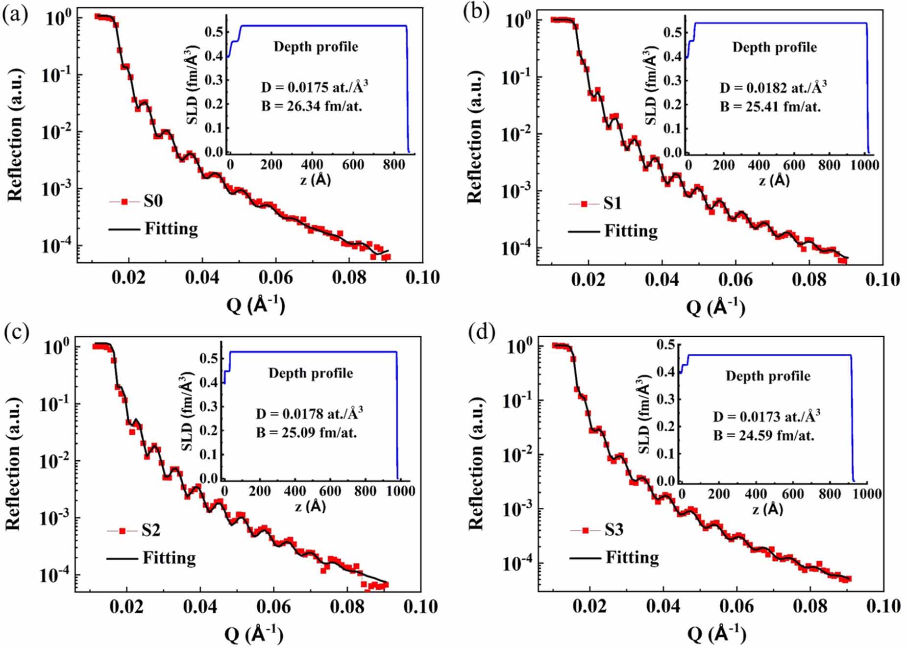
Figure 2. Experimental NR spectra and the corresponding fitting curves of all samples.
-
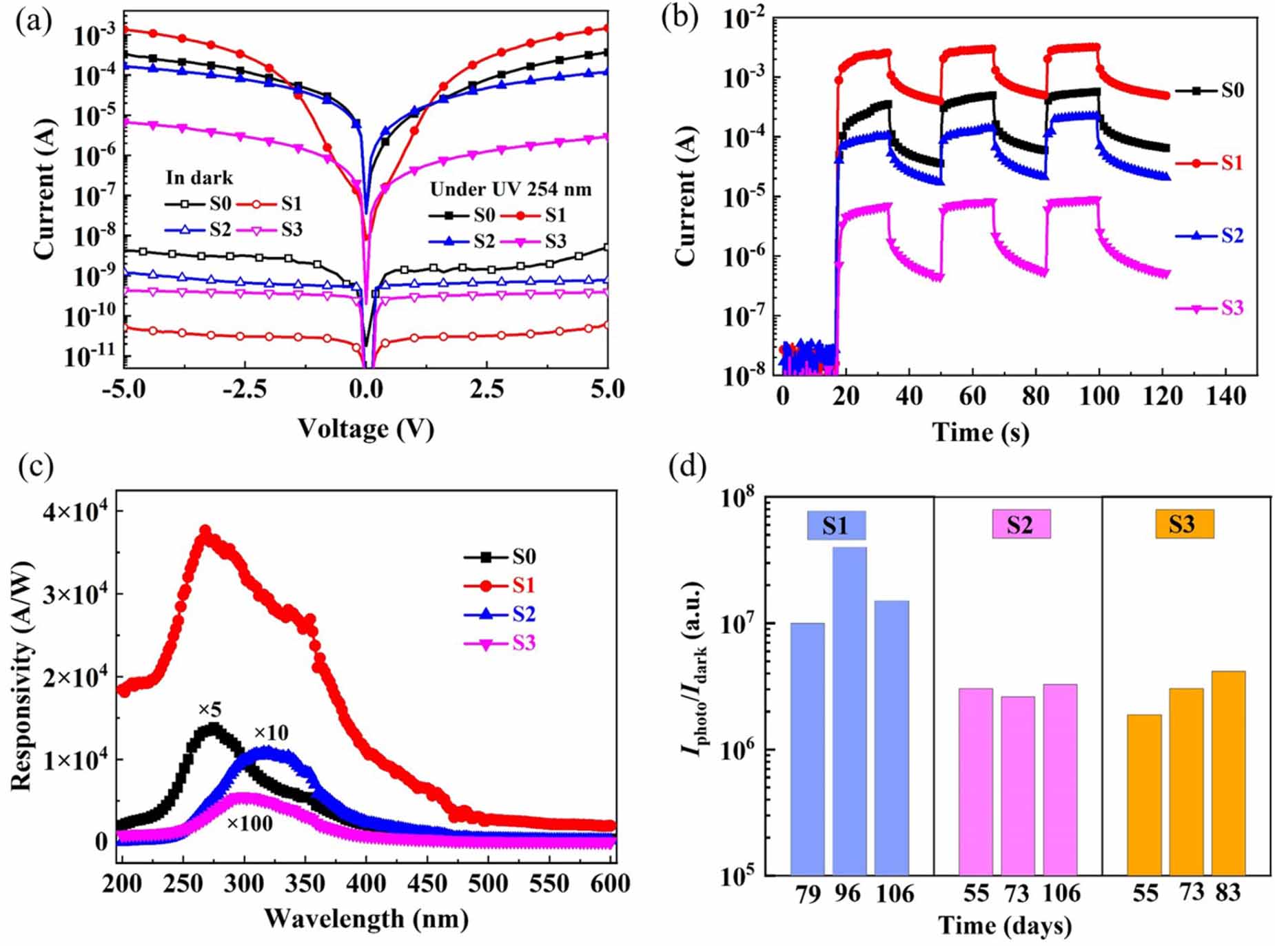
Figure 3. (a) The I-V curves in dark and under UV 254 nm light illumination. (b) Time-dependent photo-response of S0-S3 with the UV 254 nm light on and off at 10 V bias. (c) The photoresponsivity spectra of representative devices on sample S0-S3. (d) PDCR stability test within 3 months.
-
-
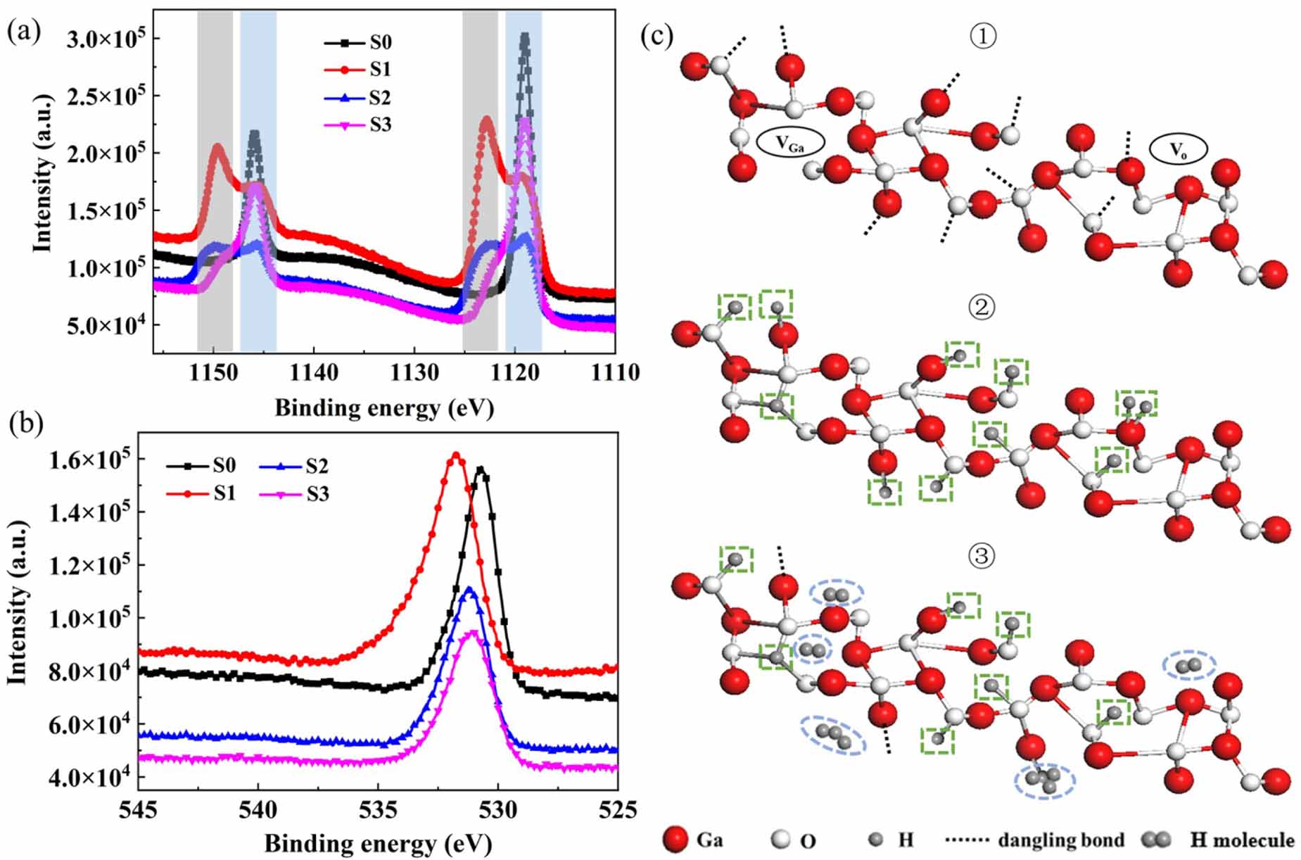
Figure 5. XPS curves of (a) Ga 2p and (b) O 1s for samples S0-S3. (c) A schematic diagram of the chemical bonds in a-Ga2O3 thin films deposited with different hydrogen fluxes. ① Initial a-Ga2O3 structure with random tilted chemical bonds, Ga/O vacancies and dangling bonds; ② with hydrogen flux of 0.5 sccm, most of the dangling bonds have been effectively passivated. ③ With higher hydrogen flux, the passivation effect is weakening due to the escape of H2 molecules.
-
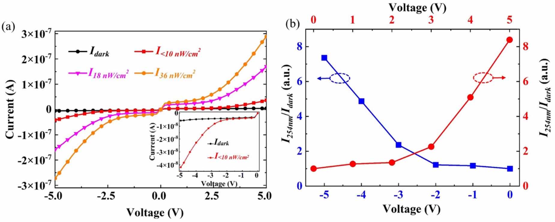
Figure 6. (a) I-V curves of S1 in dark and under UV 254 nm light illumination with different intensities. The inset is the enlarged negative part of the I-V curves in dark and under the weakest light illumination. (b) The variation of PDCR against the bias voltage for S1 sample under illumination lower than 10 nW cm-2.
-
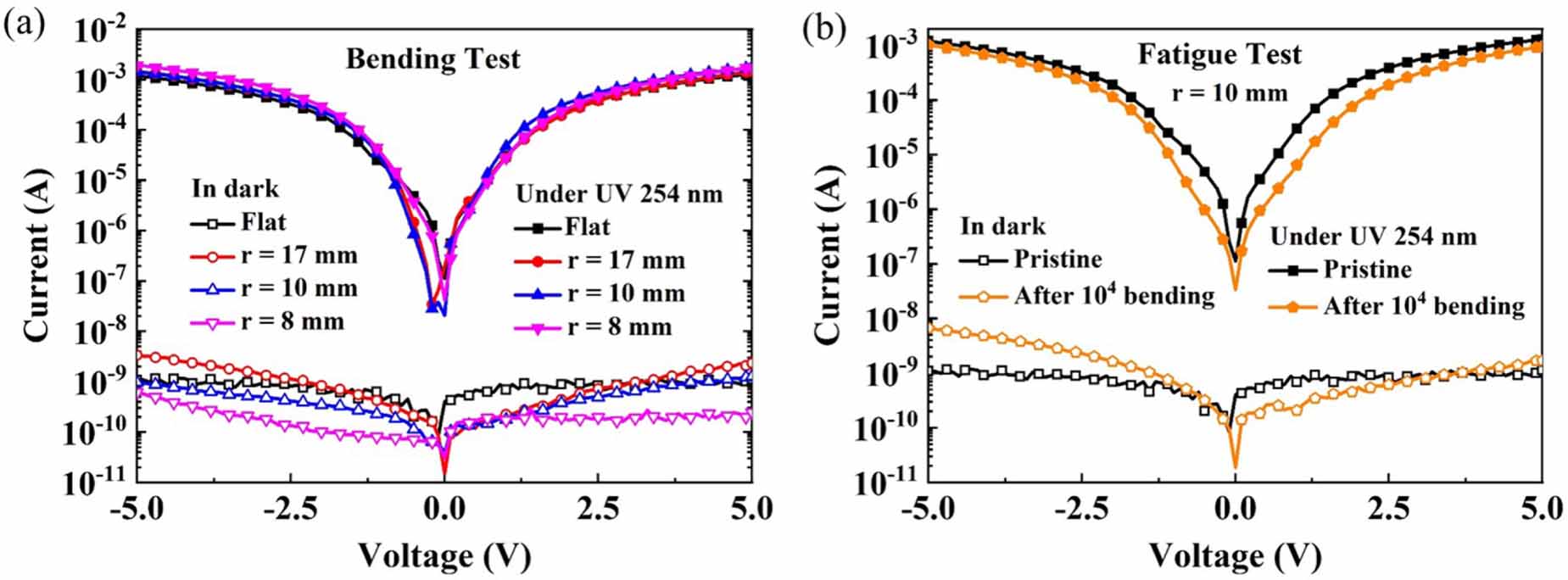
Figure 7. (a) I-V curves of P1 in dark and under 254 nm UV light illumination at flat and different bending states. (b) I-V curves of P1 in dark and under 254 nm UV light illumination before and after bending 10 000 cycles with r = 10 mm.
Figure
7 ,Table
1 个