-
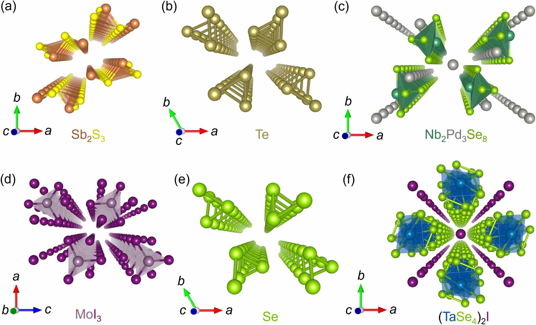
Figure 1. Crystal structures of some typical 1D vdWMs. (a) Sb2S3. (b) Te. (c) Nb2Pd3Se8. (d) MoI3. (e) Se. (f) (TaSe4)2I. The members from the 1D vdWM family typically possess strong covalent bonds in only one direction, while being combined together by weak covalent/ionic bonds or van der Waals interactions in the other two directions.
-
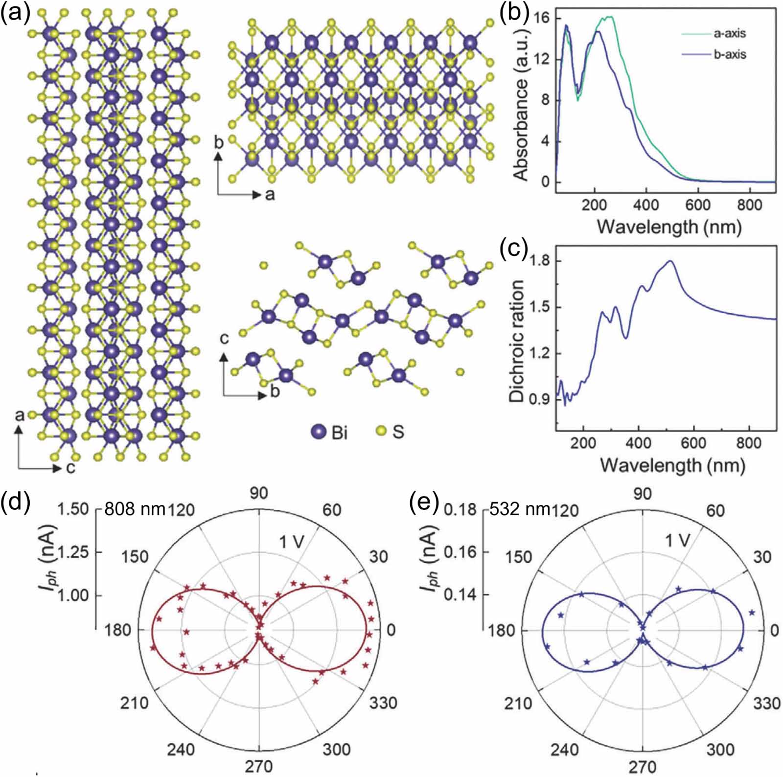
Figure 2. (a) Schematic diagrams of the crystal structure of Bi2S3 viewed from various perspectives. (b) Calculated absorbance of Bi2S3 along a-axis (green line) and b-axis (blue line). (c) The corresponding linear dichroic ratio as a function of wavelength of the Bi2S3 crystal deduced from the absorbance. (d)-(e) Polar plots of the polarization angle-resolved photocurrent of the Bi2S3 nanowire device under 808 and 532 nm illuminations, respectively. The solid lines are the fitting results using the sinusoidal function. Reproduced from [81].
CC BY 4.0 . -
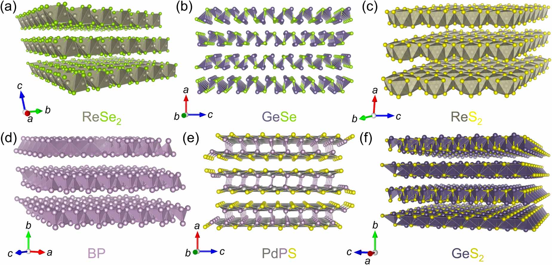
Figure 3. Crystal structures of some typical low-symmetry 2D vdWMs. (a) ReSe2. (b) GeSe. (c) ReS2. (d) Black phosphorus. (e) PdPS. (f) GeS2.
-
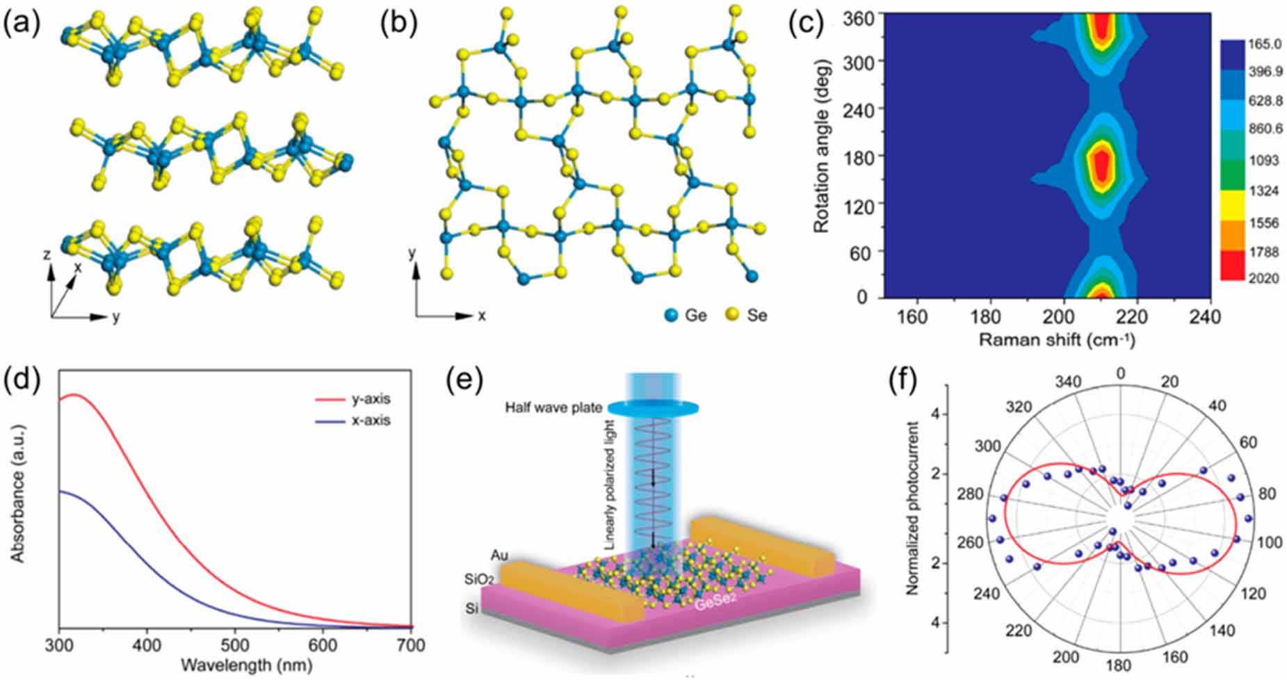
Figure 4. (a) Side view and (b) top view of the crystal structure of GeSe2. (c) Polarization angle-resolved Raman spectra of a GeSe2 nanosheet. (d) Theoretically calculated light absorption spectra along the x direction (blue line) and the y direction (red line). (e) Schematic diagram of the GeSe2 nanosheet photodetector and the measurement configuration for evaluating polarized photosensitivity. (f) Polar plot of the polarization angle-resolved photocurrent in a normalized way. Reprinted with permission from [120]. Copyright (2018) American Chemical Society.
-
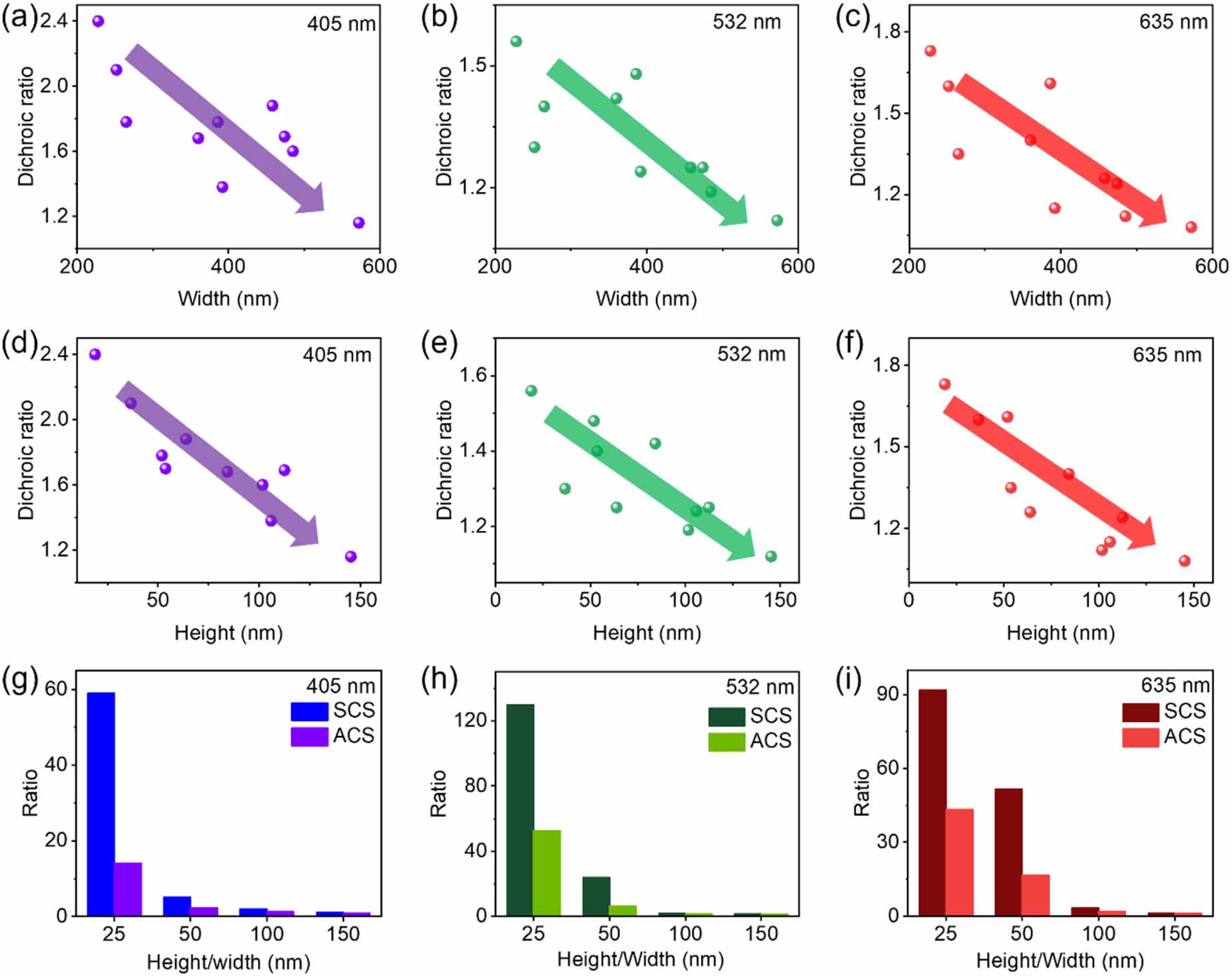
Figure 5. (a)-(c) Linear dichroic ratio as a function of the channel width upon 405, 532, and 635 nm illuminations. (d)-(f) Linear dichroic ratio as a function of the channel height upon 405, 532, and 635 nm illuminations. (g)-(i) Anisotropic ratios of ACS (purple columns) and SCS (blue columns) as a function of the width/height of the Bi2S3 nanowire upon 405 nm, 532 nm, and 635 nm excitations. Reproduced from [97] with permission from the Royal Society of Chemistry.
-

Figure 6. (a) Schematic illustration of the SbI3/Sb2O3 core-shell heterojunction. The bottom images present the crystal structures of SbI3 (left) and Sb2O3 (right). (b) The theoretical absorbance curves along a-axis (solid lines) and b-axis (dashed lines) of the SbI3/Sb2O3 heterostructure, SbI3, and Sb2O3, respectively. (c) The corresponding linear dichroic ratio as a function of wavelength of the SbI3/Sb2O3 core-shell heterostructures (blue line), SbI3 (red line), and Sb2O3 (orange line). (d) Polar plots of the polarization angle dependent photocurrent upon 450 nm (blue stars) and 532 nm (red stars) illuminations. The blue and red lines are fitting curves by the function of Iph = Ipx cos2(
+ ) + Ipysin2( + ). (e) Polarization angle dependent photocurrent upon 450 and 532 nm illuminations in an orthogonal coordinate. [185] John Wiley & Sons. © 2020 WILEYVCH Verlag GmbH & Co. KGaA, Weinheim. -
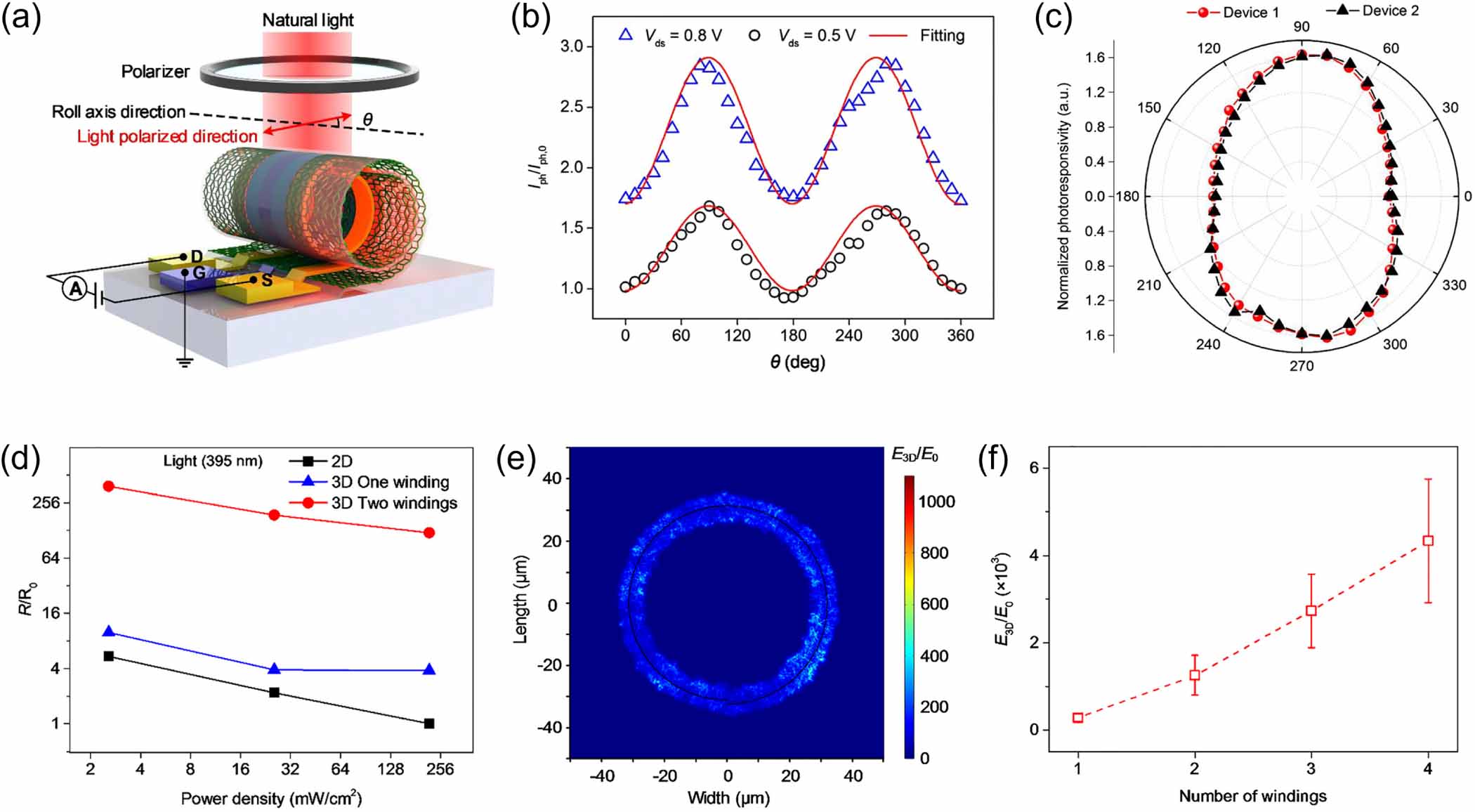
Figure 7. (a) Schematic diagram of a 3D MoS2 phototransistor for polarization-discriminating photodetection. The polarization angle (
) is defined as the angle between the polarization direction of linearly polarized incident light and the axial direction of the MoS2 roll. (b) Normalized polarization angle dependent photocurrent of a 3D MoS2 phototransistor under different source-drain voltages, where Iph,0 represents the photocurrent measured under the polarization angle of 0. (c) The corresponding polar plots of the data in (b). (d) Responsivity as a function of light power density of 2D MoS2 photodetector (black line) and 3D MoS2 photodetectors with one winding (blue line) and two windings (red line). (e) The spacial distribution of the electric field magnitude in vicinity of a 3D MoS2 roll with one rolled-up winding under 395 nm illumination. (f) The average normalized electric field magnitude (E3D/E0) at the surface of 3D MoS2 rolls with various rolled-up windings. Reproduced from [195]. CC BY 4.0 . -
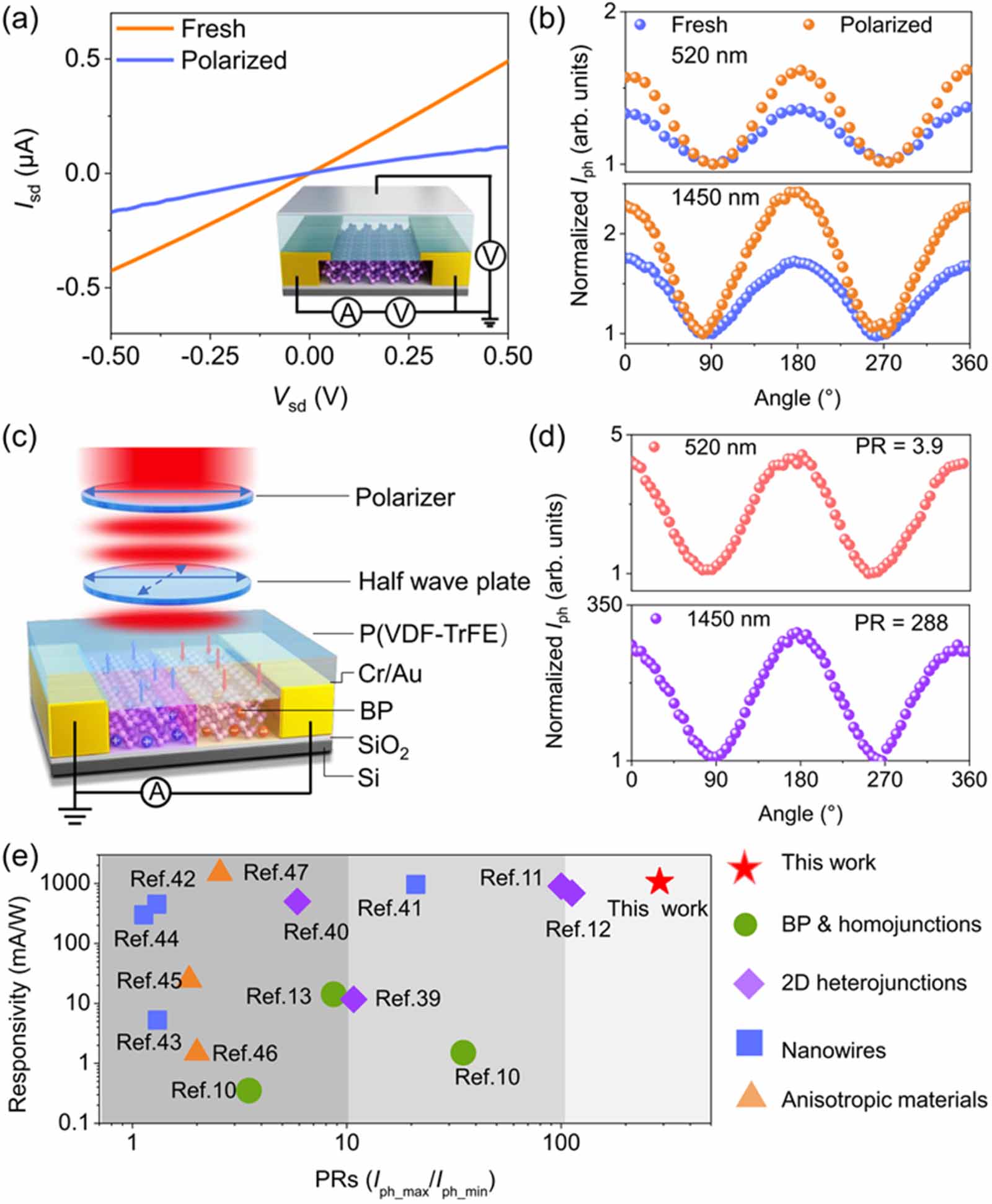
Figure 8. (a) Output characteristics of the pristine (orange line) and polarized (blue line) black phosphorus phototransistors. The inset presents the device structure. (b) Normalized photocurrent of the device at the fresh (blue dots) and polarized (orange dots) states as a function of the polarization angle upon 520 (top panel) and 1450 (bottom panel) nm illuminations, respectively. (c) Schematic of black phosphorus in-plane p-n homojunction defined by ferroelectric domains. (d) Normalized photocurrent of the black phosphorus in-plane p-n homojunction as a function of the polarization angle upon 520 and 1450 nm illuminations, respectively. Polarization ratio (PR) is defined as the ratio of the maximum photocurrent to the minimum photocurrent. (e) Responsivity and PR of black phosphorus in-plane p-n homojunction defined by ferroelectric domains compared with black phosphorus, black phosphorus homojunctions defined by other methods, 2D heterojunctions, nanowires, and other anisotropic materials, showing that this work is at the leading level among most of the previously reported polarization photodetectors. Reproduced from [208].
CC BY 4.0 . -
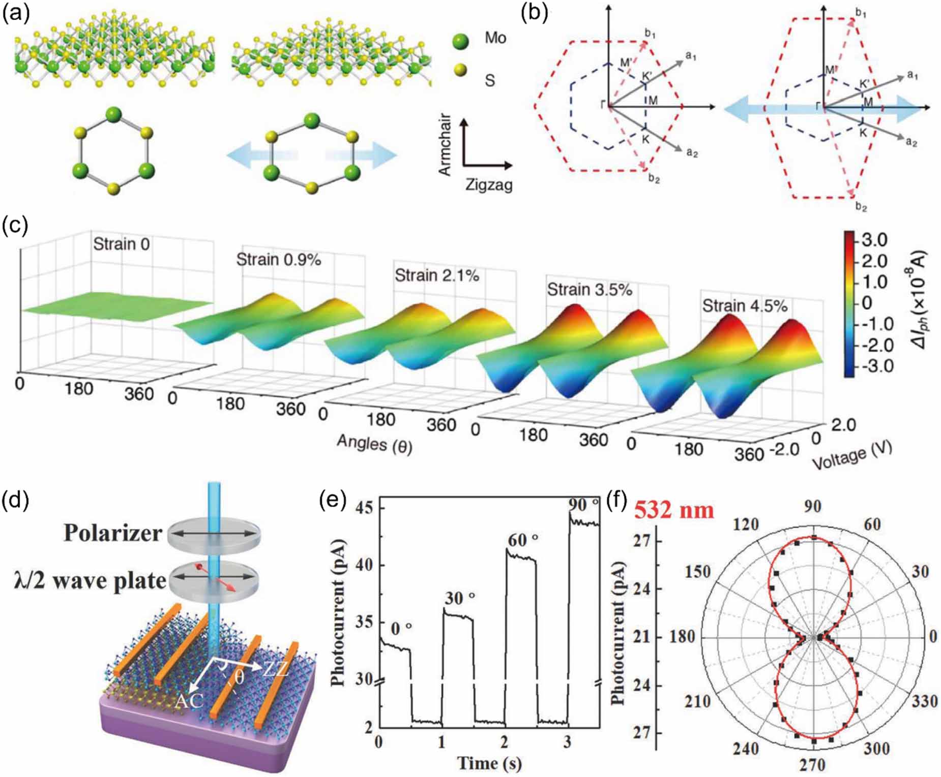
Figure 9. (a) Comparison of the in-plane crystal structures of pristine MoS2 and MoS2 upon external tensile strain. (b) The Brillouin cells of pristine MoS2 and MoS2 upon external tensile strain. (c) Polarization angle-resolved photocurrent of a MoS2 photodetector under various strain values. Reprinted from [235], © 2019 Elsevier Ltd. All rights reserved. (d) Schematic diagram of the WSe2/CrOCl photodetector. (e) Photoswitching curves of the WSe2/CrOCl device under 532 nm illuminations with different polarization angles. (f) Polar plot of the photocurrent as function of polarization angle under 532 nm illumination. [236] John Wiley & Sons.© 2022 WileyVCH GmbH.
-
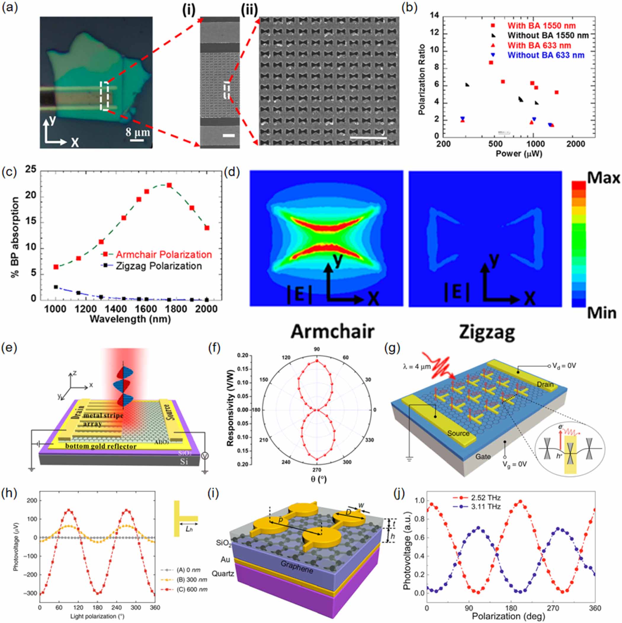
Figure 10. (a) Optical image and SEM images of a black phosphorus photodetector integrating a bowtie aperture array. (b) Polarization ratio as a function of light power of black phosphorus photodetectors with and without bowtie apertures upon 633 and 1550 nm illuminations. (c) Computed absorption as a function of wavelength along the armchair and zigzag directions of black phosphorus integrated with bowtie apertures. (d) Top view of the electric field distribution in vicinity of a bowtie aperture under illuminations along the armchair (left) and zigzag (right) directions, respectively. Reprinted with permission from [252]. Copyright (2018) American Chemical Society. (e) Schematic depiction of a graphene phototransistor with integrated plasmonic cavity. (f) Polarization angle dependent photoresponse in a polar plot of the graphene phototransistor integrated with plasmonic cavity under 1550 nm illumination. Reprinted from [253], with the permission of AIP Publishing. (g) 3D schematic diagram of a metasurface-mediated graphene photodetector. (h) Polarization angle dependent photovoltage of graphene photodetectors with metasurfaces of various geometries. Reproduced from [257].
CC BY 4.0 . (i) Schematic illustration depicting the graphene photodetector integrated with monolithic metamaterial. (j) Polarization angle dependent photovoltage upon illuminations with frequencies of 2.52 and 3.11 THz. Reprinted with permission from [259]. Copyright (2022) American Chemical Society. -
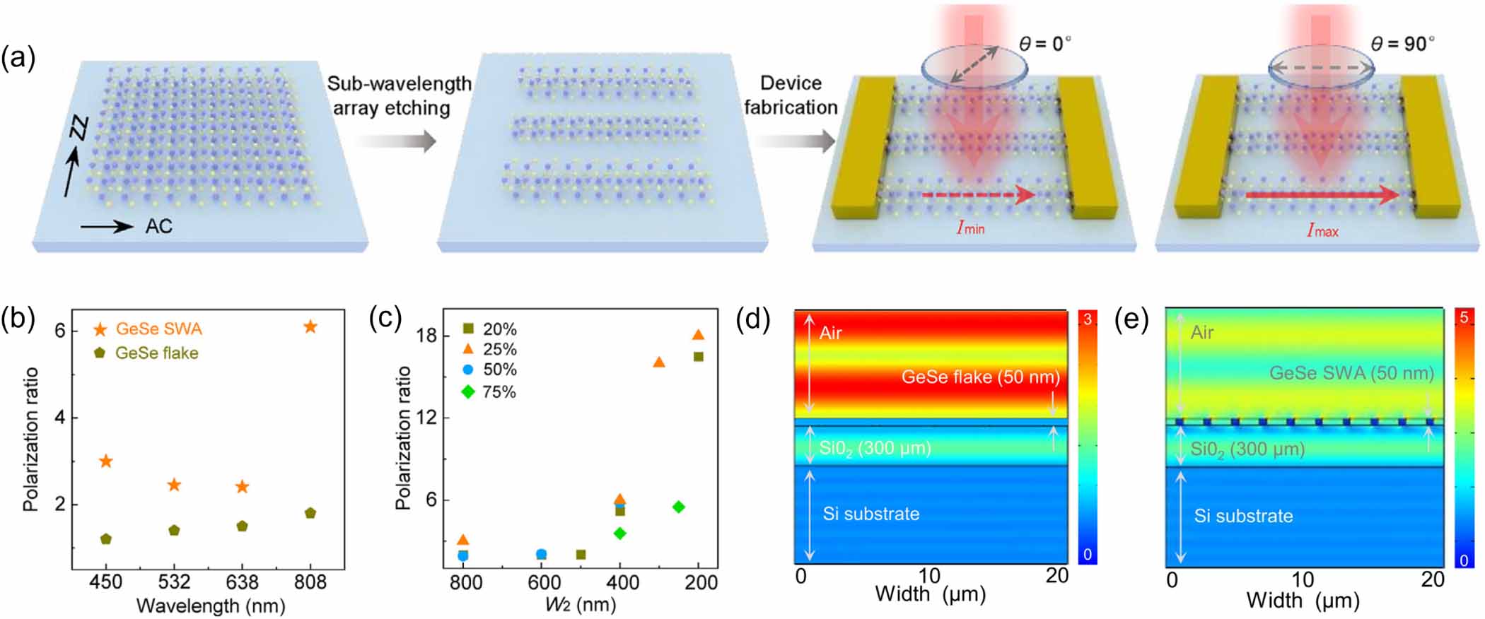
Figure 11. (a) Schematic diagram depicting the fabrication process of the GeSe sub-wavelength array photodetector and the measurement configuration. (b) Linear dichroic ratios of the pristine GeSe photodetector and the GeSe sub-wavelength array photodetector upon illuminations with various wavelengths. (c) Linear dichroic ratio as a function of period width with a series of nanostrip width/period width ratios. Calculated electric field intensity distribution of light of (d) the pristine GeSe flake and (e) the GeSe sub-wavelength array upon 800 nm irradiation. Reprinted from [264],© 2023 Science China Press. Published by Elsevier B.V. and Science China Press. All rights reserved.
-
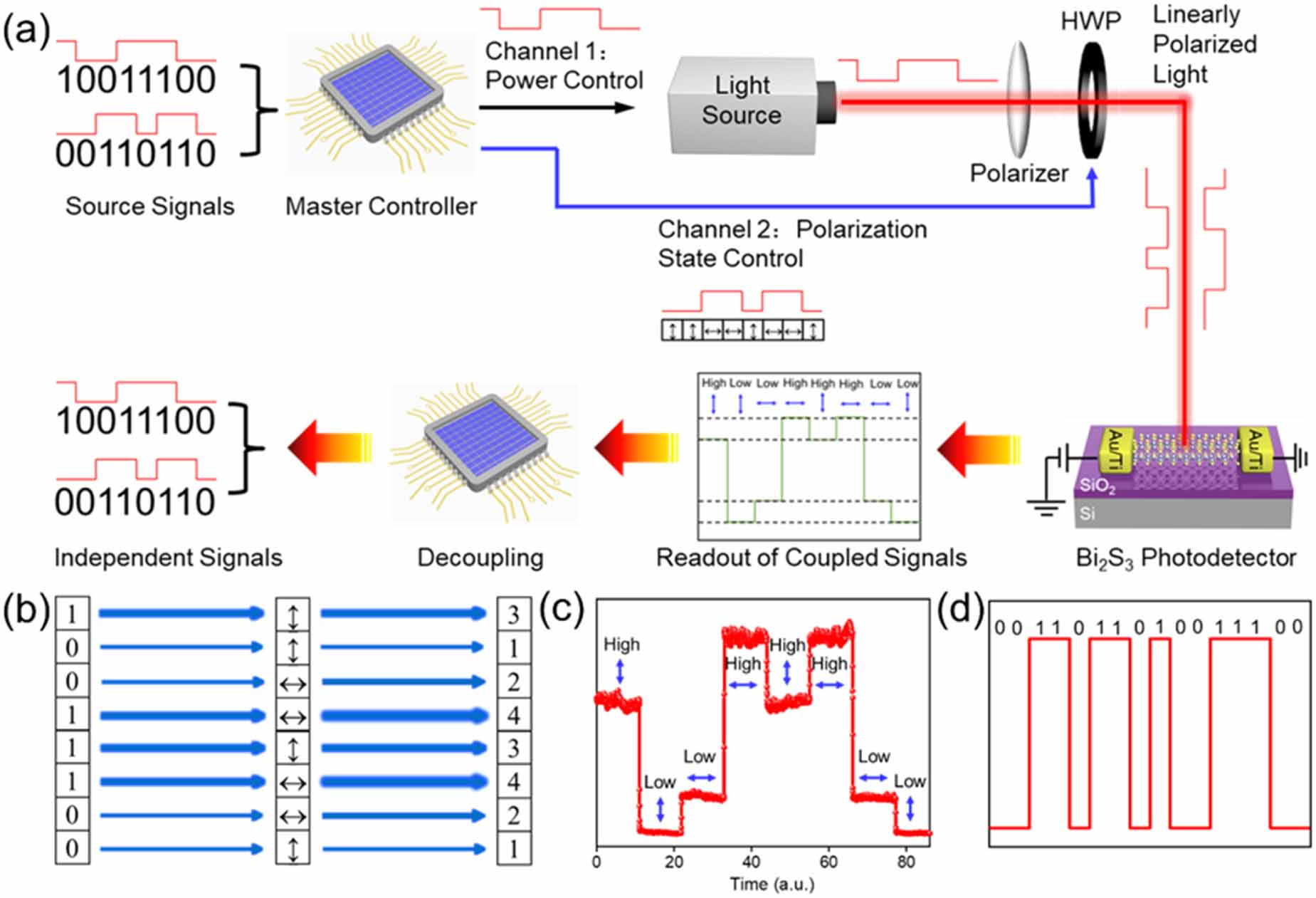
Figure 12. (a) Schematic diagram illustrating the principle of multiplexing optical communications based on a polarization-discriminating Bi2S3 nanowire photodetector. (b) Schematic diagram of the input light intensity signal and the corresponding polarization state signal from the signal output end. The
-
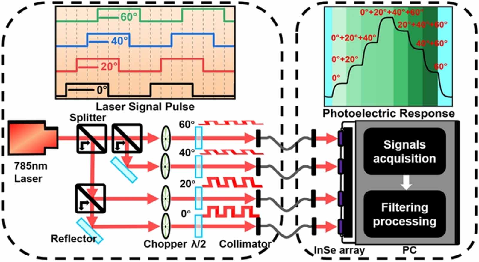
Figure 13. Schematic illustration of the polarization division multiplexing approach for optical communications based on the polarized -InSe photodetectors. Reproduced from [272].
CC BY 4.0 . -

Figure 14. Contrast-enhanced polarization imaging based on Te photodetectors. (a) Schematic illustration of the imaging configuration based on a Te photodetector. (b) Schematic of the polarization imaging mechanism for extract the degree of linear polarization (DoLP). (c) Normalized imaging contrast of S0 and DoLP by using various devices as light-sensing units. (d) Imaging DoLP result using the nonpolarized 2H-MoTe2 device upon 1.55 m illumination. (e)-(f) Imaging DoLP results using the Te photodetector upon 1.55 and 2.3 m illuminations, respectively. Reproduced from [277].
CC BY 4.0 .
Figure
14 ,Table
3 个