-
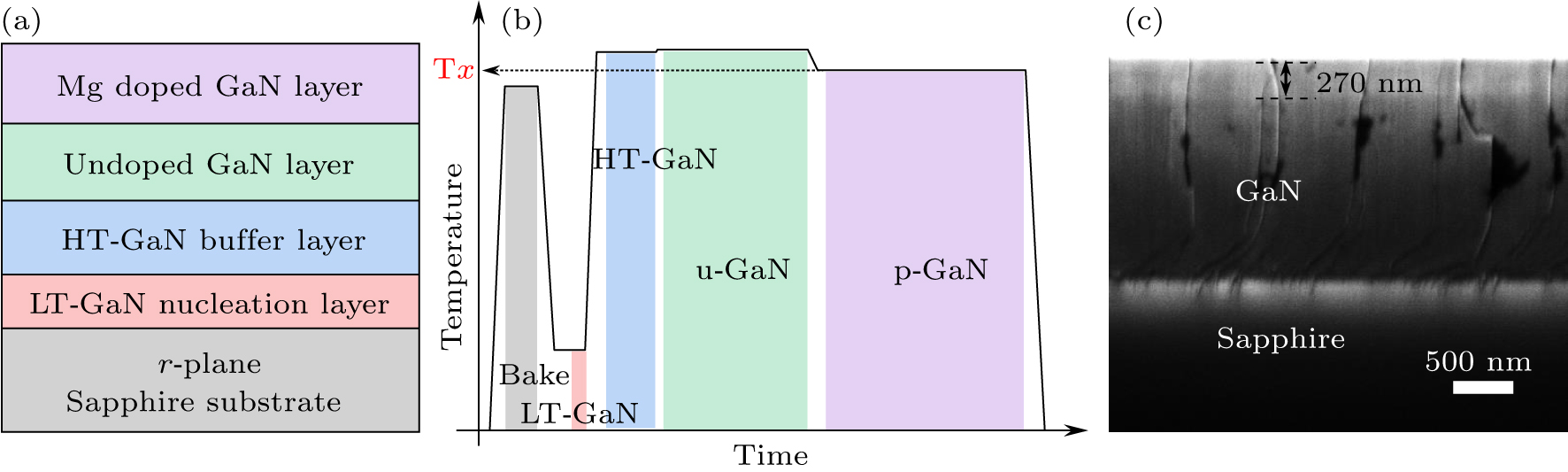
Figure 1. (a) The schematic layer structure for the nonpolar a-plane p-type GaN samples. (b) The growth temperature of each layer varies with time. (c) The cross-sectional SEM graph for the nonpolar a-plane p-GaN sample.
-
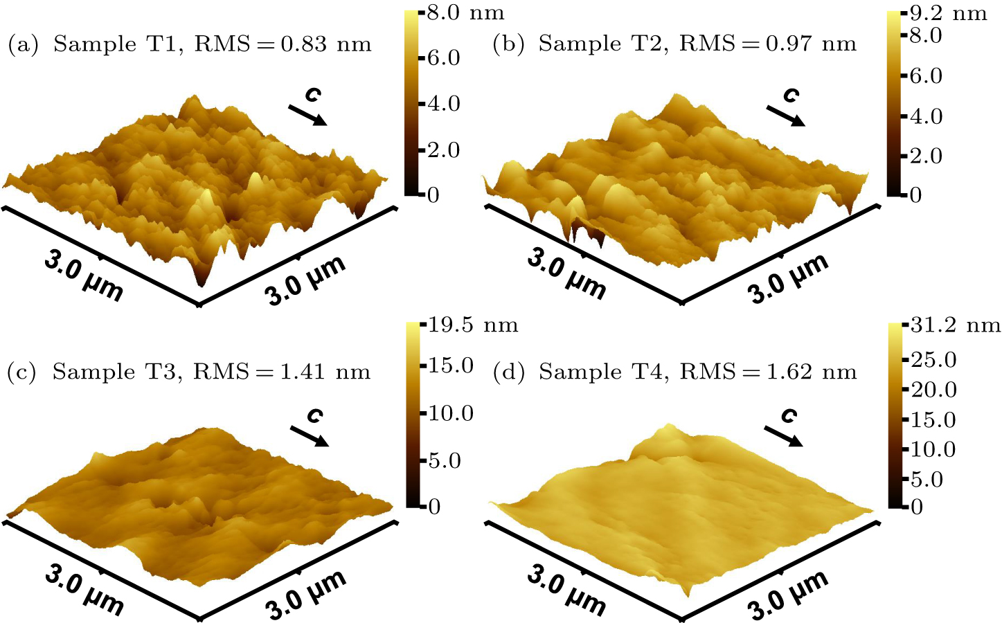
Figure 2. (a)–(d) The AFM images for the samples T1–T4 with a detection area of 3 μm × 3 μm.
-
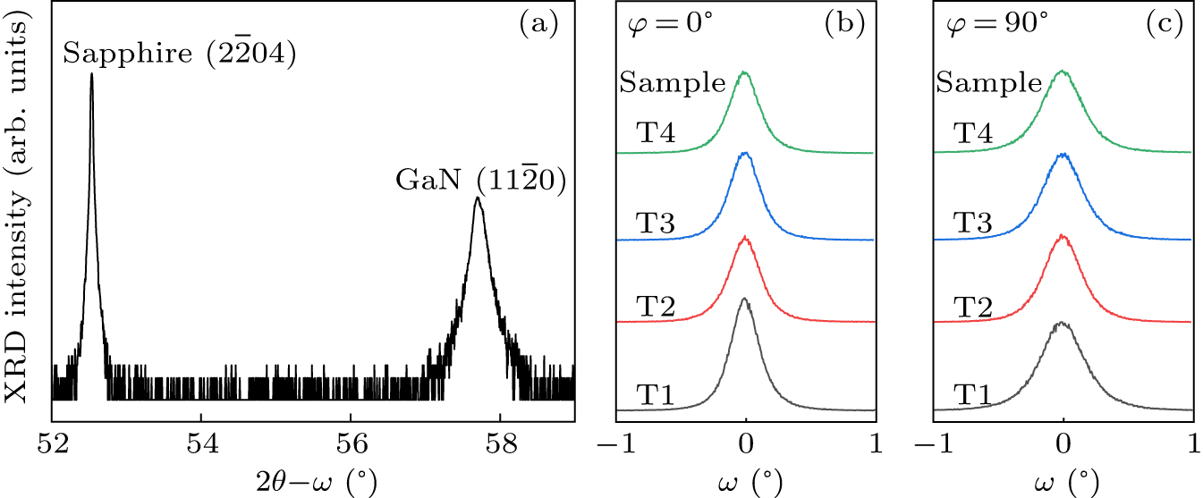
Figure 3. (a) The XRD ω–2θ scanning curve for the nonpolar a-plane p-type GaN. (b) XRCs of the samples T1–T4.
-
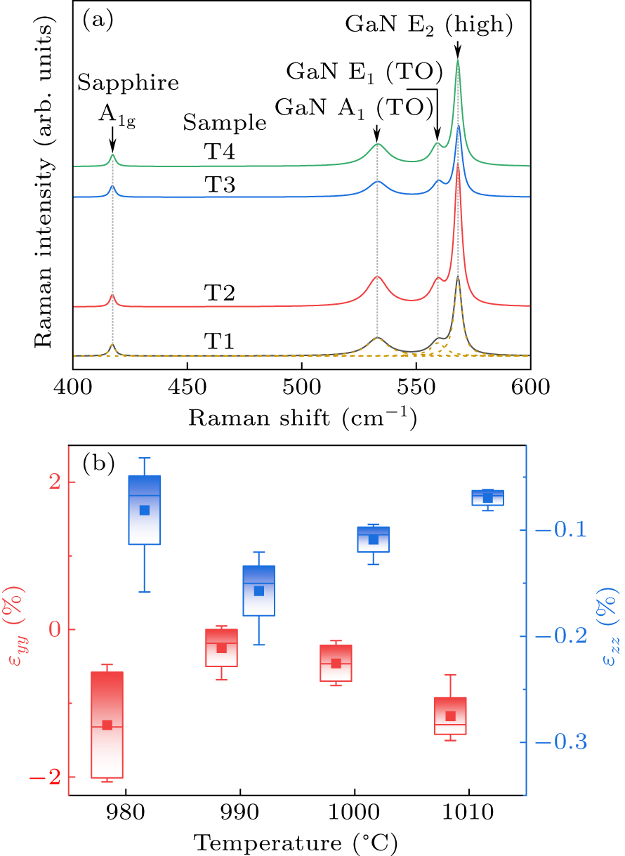
Figure 4. (a) Raman spectra and (b) calculated in-plane strains of samples T1–T4.
-
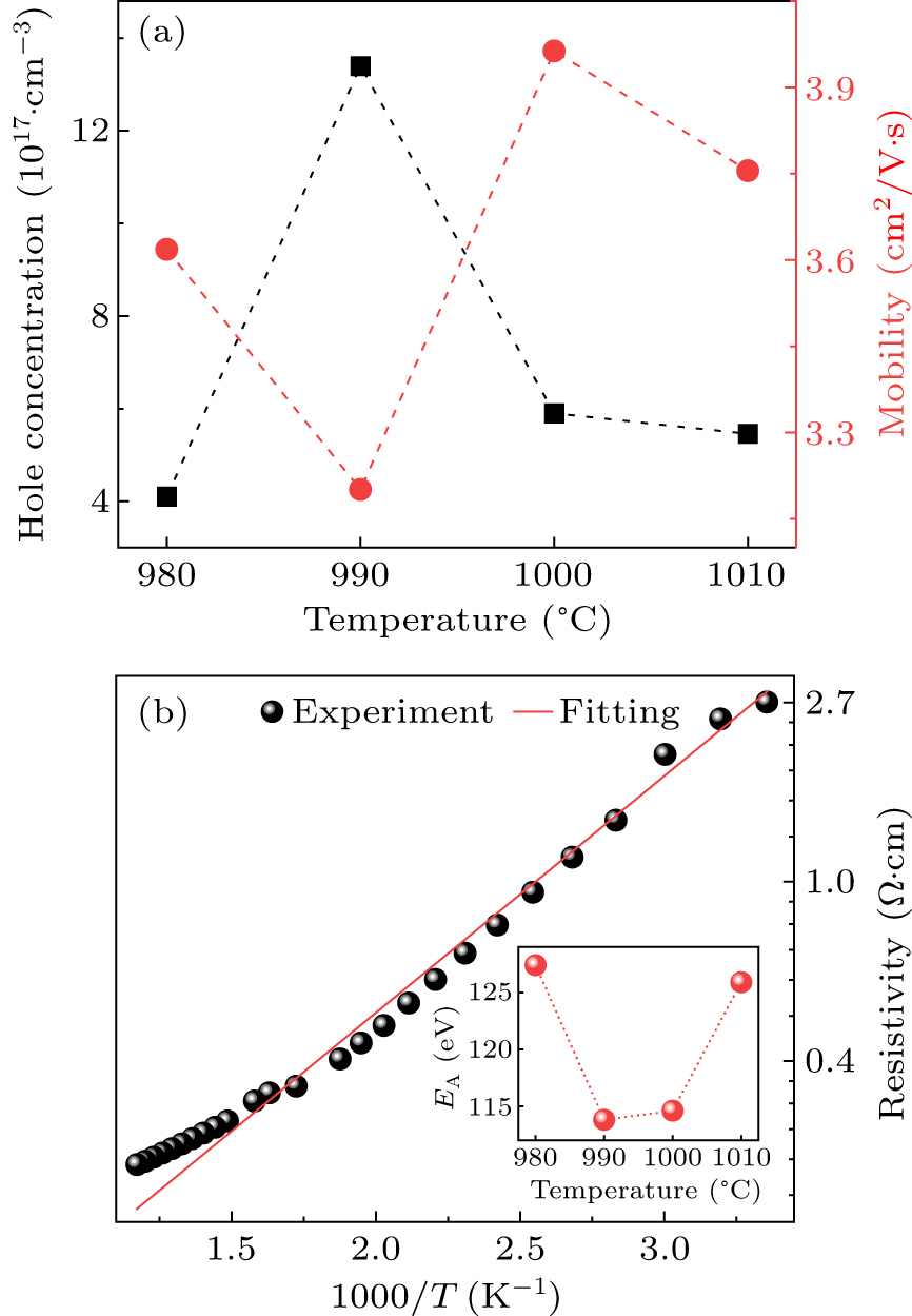
Figure 5. (a) The AC Hall effect measurement at room temperature for sample T1–T4. (b) The resistivity for sample T2 as a function of reciprocal temperature. The inset is the acceptor activation energy of samples T1–T4.
-
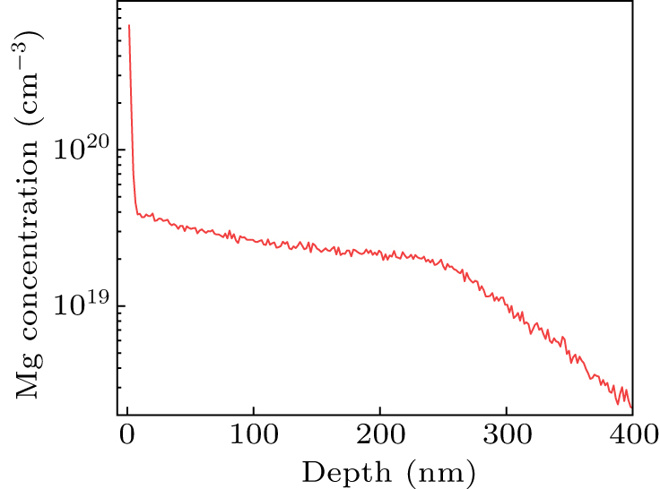
Figure 6. SIMS measurement of sample T2.
Figure
6 ,Table
1 个