-
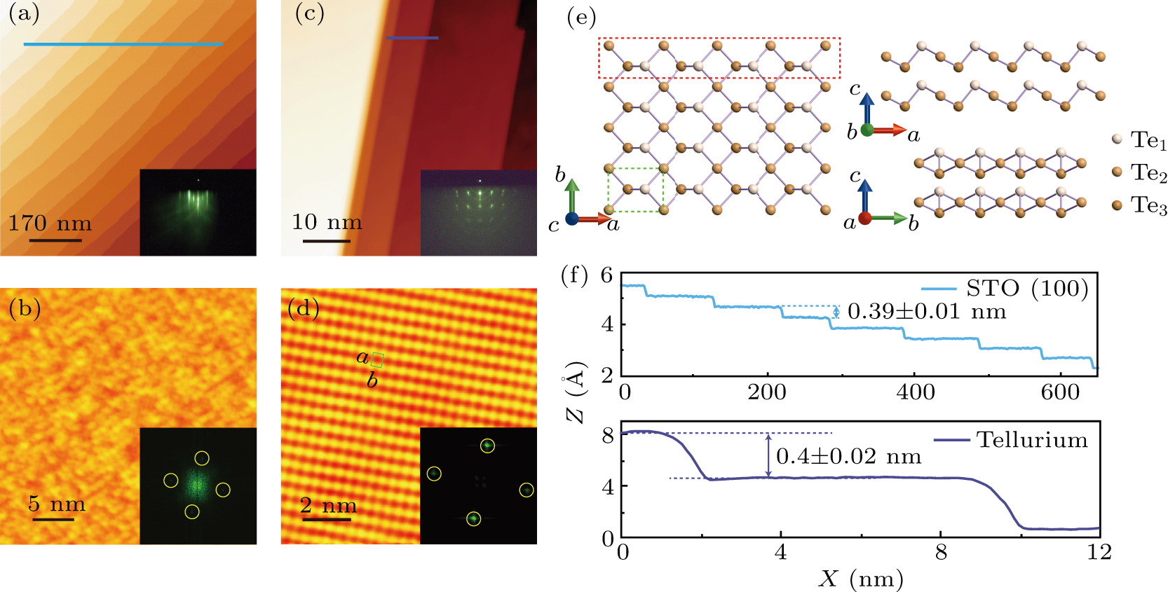
Figure 1. High-temperature growth of ultra-thin Te films on STO (001) substrate. (a) Large-area STM image of STO (001) surface (U = +3 V, It = 10 pA). The inset is the RHEED pattern of the substrate. (b) The high-resolution STM image of the substrate (U = +1 V, It = 10 pA). The inset shows the FFT pattern. (c) STM image of the HT-grown (80 °C) β-Te films (U = +3 V, It = 10 pA). The inset shows the RHEED pattern of the films. (d) The atomically resolved STM images (U = +2 V, It = 50 pA) of the HT-grown films. The insert is the FFT pattern. (e) The lattice structure of β-Te. (f) Section profiles of (a) and (c).
-
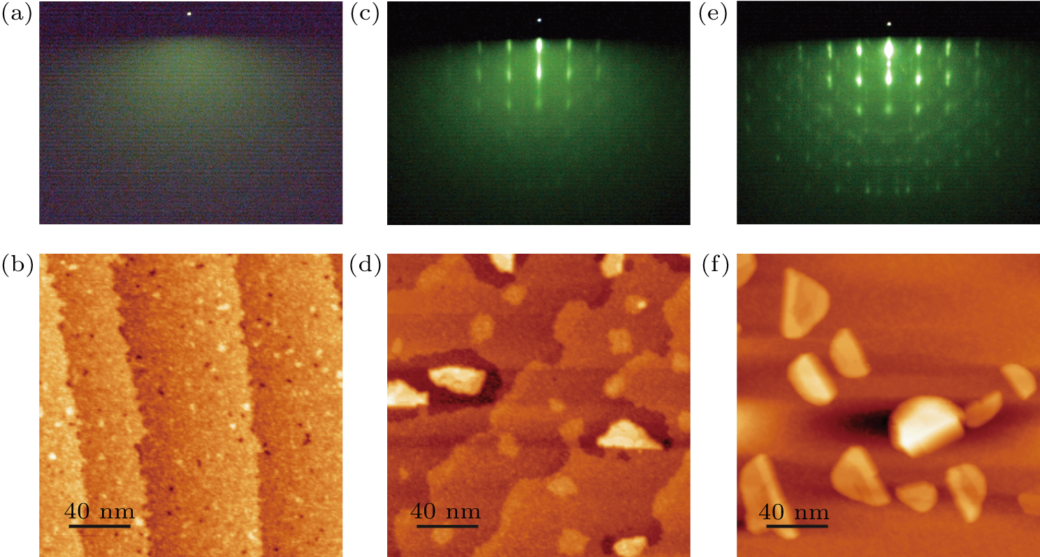
Figure 2. The RHEED patterns and STM morphologies of Te films (2 ML) at different growth steps. (a) and (b), (c) and (d), (e) and (f) are for films (2 ML) after LT, after FA around Td, and after annealing (80 °C) for 10 min, respectively.
-
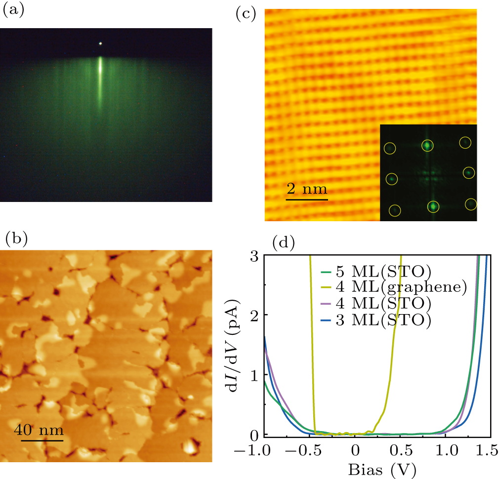
Figure 3. LT growth of 3 ML Te films on STO (001) substrate and the band gap evolution of β-Te films with different thicknesses. (a) and (b) The RHEED pattern and STM morphology (U = +3 V, It = 10 pA) of 3-ML β-Te after the LT/FA process, respectively. (c) The corresponding atomically resolved STM images (U = +2 V, It = 50 pA). The inserts display the FFT pattern. (d) STS spectra measured on films with various thicknesses on STO and graphene.
-
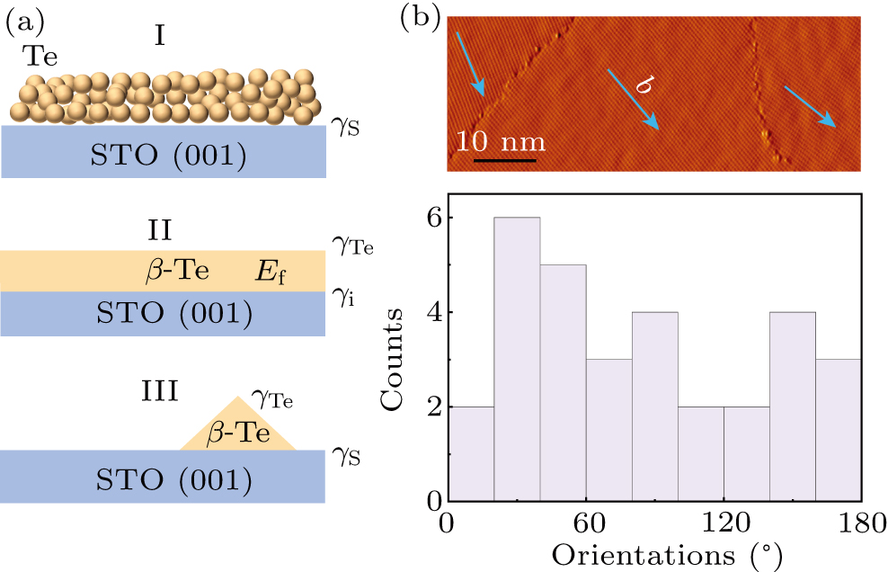
Figure 4. (a) Schematic of thermodynamic conditions of the Te-growth on STO. (b) The domain orientations of β-Te films. The upper part represents the morphology of different orientation domains of the 3-ML β-Te films (U = +3 V, It = 50 pA), and the lower part is a statistical histogram of domain orientations with respect to that of the substrate.
Figure
4 ,Table
0 个