-
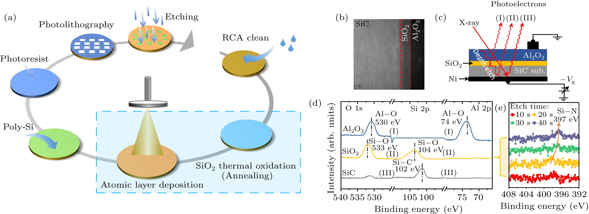
Figure 1. ALD Al2O3 stacked on nitride SiO2. (a) Schematic process of the MOS capacitors poly-Si/Al2O3/SiO2/SiC/Ni. (b) Transmission electron microscopy (TEM) image of the prepared MOS stack. (c) Schematic illustration of the MOS sample measurement by XPS. XPS spectrum for the MOS stack: (d) XPS carried on the Al2O3, SiO2 and SiC films for special positions at O 1s, Si 2p and Al 2p; (e) XPS carried on the cross depth of SiO2 films by controlling plasma etching time from 10 s to 40 s at N 1s binding position.
-
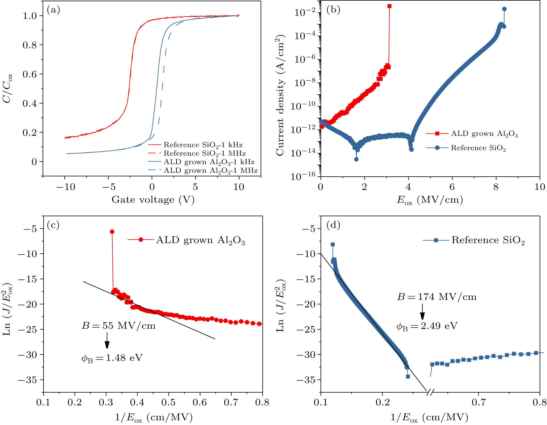
Figure 2. Interfacial state defects and dielectric breakdown characteristics of pure SiO2 and Al2O3 dielectric MOS capacitors. (a) HF C–V curves of MOS capacitors. (b) Room temperature (300 K) results of current density (J)–electric field (E) plots of MOS capacitors. A Fowler–Nordheim plot for pure (c) Al2O3 and (d) SiO2 dielectric MOS capacitors.
-
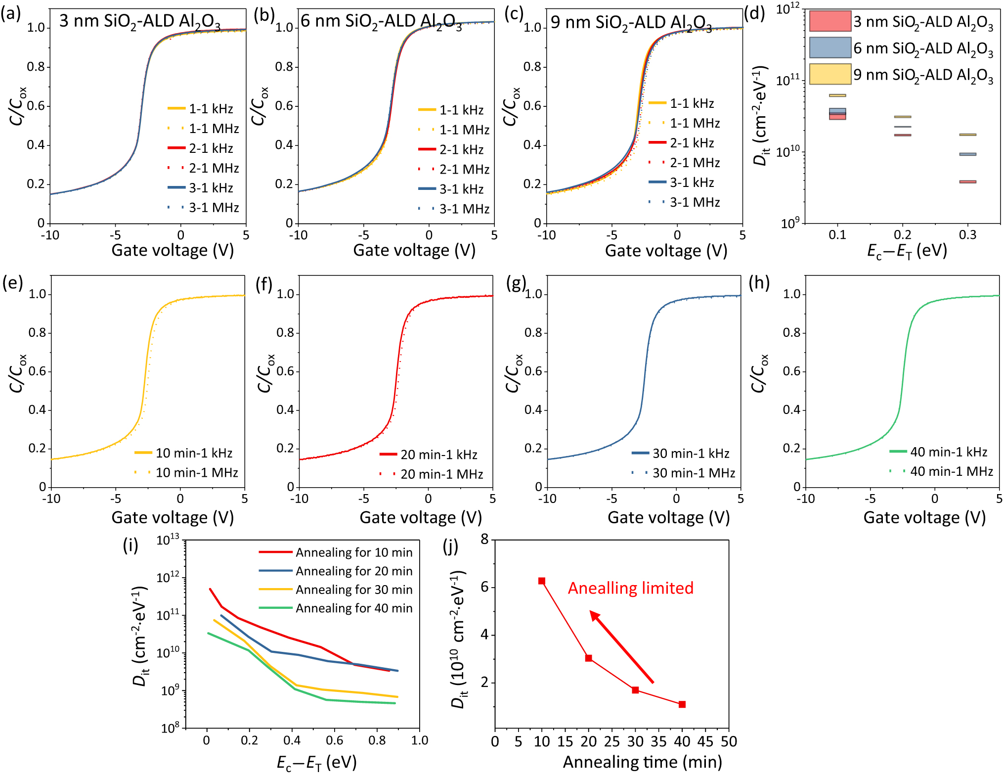
Figure 3. Interfacial characteristics for the stack Al2O3 dielectric samples grown by different thicknesses SiO2. (a)–(c) HF C–V curves of MOS capacitors for different thicknesses SiO2. (d) Density of interface states (Dit) as a function of energy from the SiC conduction band edge, extracted from C–V analysis at room temperatures for the stack Al2O3 dielectric samples grown by different thicknesses SiO2. (e)–(h) HF C–V curves of MOS capacitors with increasing annealing time. (i) Density of interface states with increasing annealing time of the SiO2 samples. (j) The density of interfacial states changes with increasing annealing time of the SiO2 samples.
-
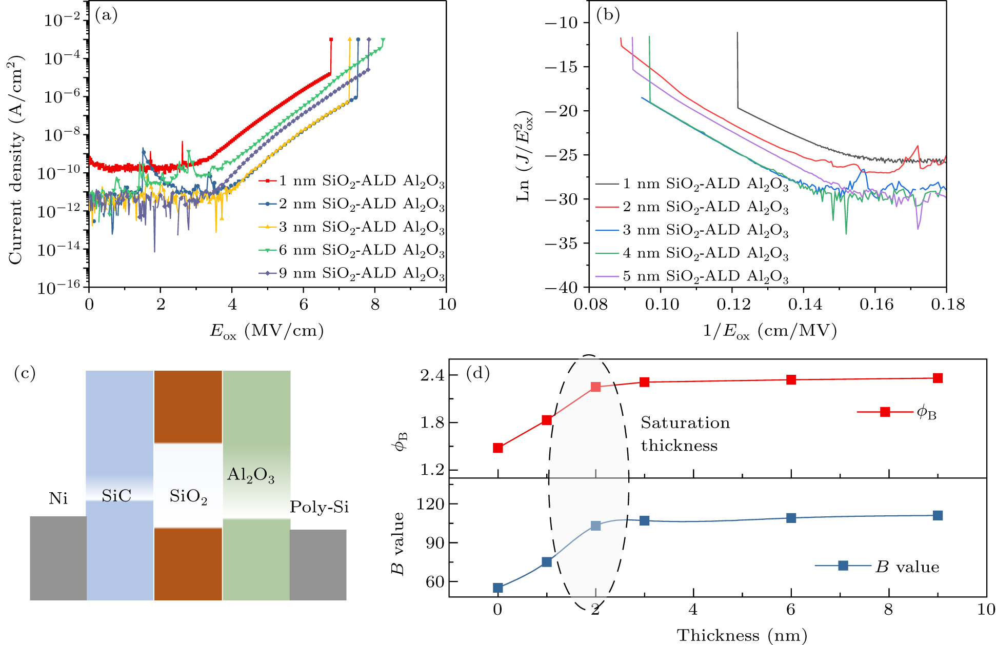
Figure 4. Dielectric breakdown characteristics of the stack Al2O3 dielectric samples grown by different thicknesses SiO2. (a) Room temperature (300 K) results of current density (J)–electric field (E) plots of MOS capacitors. (b) A Fowler–Nordheim plot for MOS capacitors. (c) Schematic band offset of the MOS capacitors Ni/SiC/SiO2/Al2O3/poly-Si. (d) Saturation thickness of stacked SiO2 in atomic-layer-deposited Al2O3 gate on 4HSiC.
Figure
4 ,Table
0 个