-
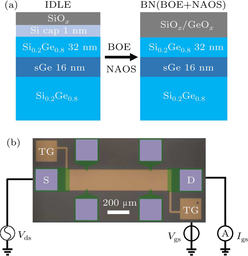
Figure 1. Ge/SiGe heterostructure and field-effect transistor (FET) device. (a) Ge/SiGe layer schematics without (left panel) and with (right panel) passivation treatment. (b) Light field pattern of Hall bar-type FET and measurement setup of FET device [TG, top gate (brown), S (D), source (drain) consists of ion implantation (green) and contact metal (silver)].
-
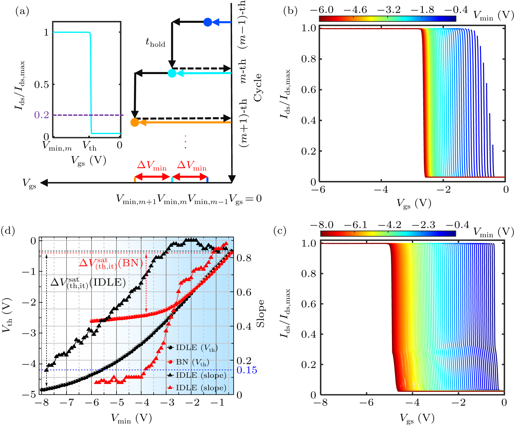
Figure 2. Cyclic scanning experiments on transfer curves. (a) Measurement process of cyclic scanning of a transfer curve. The inset shows the transfer curve during the m-th cycle scanning with Vgs scanned from 0 to Vmin, m. Here, m = 29 and Vmin,m = −3.2 V. The current is normalized to Ids/Ids,max, where Ids,max stands for the maximum current at the last cyclic scanning experiment. The purple dashed line represents the condition where the current ratio Ids/Ids,max = 0.2, and the corresponding gate voltage Vgs is defined as the threshold voltage Vth. (b) Transfer curves for Vmin decreasing from −0.4 V (blue) to −6 V (red) of the BN sample. (c) Transfer curves for Vmin decreasing from −0.4 V (blue) to −8 V (red) of the IDLE sample. (d) Threshold voltage Vth (circles) and slope of Vth (triangle) dependent on Vmin. The black and red lines correspond to the results from the IDLE sample and BN sample, respectively. The blue gradient background represents the gradual saturation process of the threshold voltages Vth (from blue to white). The blue dashed line represents a slope of 0.15, which is defined as the standard for the threshold saturation in this experiment.
-
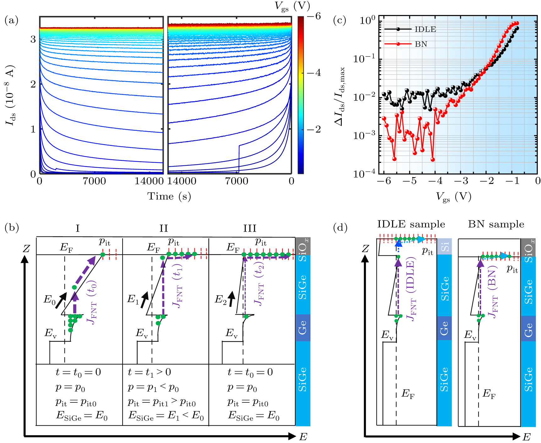
Figure 3. Time-dependent current measurement. (a) Long-term current stability at different voltages from −0.4 V to −6 V for sample BN (left panel) and sample IDLE (right panel). (b) Energy levels at different times under a fixed gate voltage, corresponding to one of the colored curves in panel (a). Panels I to II represent a rapid decay process. Panels II to III represent a long-tail decay process. The solid green circles represent holes. The solid red line (dashed line) represents interface states with (without) holes filled, while the purple dashed arrow lines represent the FNT current JFNT, with varying widths indicating different magnitudes of JFNT. The black dashed line represents the Fermi level within the semiconductor. E0,1,2 represents the electric field strengths in the SiGe barrier at three different times t0,1,2. Additionally, Z represents the sample growth direction and E indicates the direction of increasing hole potential. (c) Normalized current decay in IDLE and BN samples at different gate voltages. (d) Schematic diagram of the process in which holes in the QW are captured by surface defects in IDLE and BN samples, respectively. The purple, blue and light blue dashed arrows represent the FNT process through the SiGe barrier layer, direct tunneling through the Si cap layer and the surface defect capture process, respectively.
Figure
3 ,Table
0 个