-
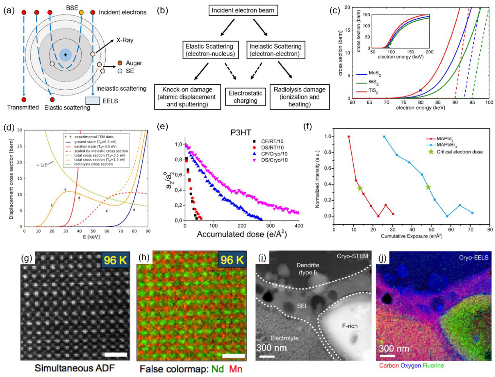
Figure 1. Electron-material interactions and Cryo-TEM capabilities. (a) Schematic diagram of the incident electron beam interacting with an atom, illustrating the nucleus and electron shells. Elastic scattering (left) and inelastic scattering (right) are depicted. BSE, backscattered electron; SE, secondary electron; EELS, electron energy-loss spectroscopy. (b) Classification of electron beam-induced damage according to scattering type. (c) Calculated sputtering cross-section for sulfur atom from MoS2, WS2 and TiS2 monolayers. Reproduced with permission from Ref. [30]. (d) Displacement cross-sections (σ) of S atoms in MoS2 (squares) and theoretical curves. Reproduced with permission from Ref. [32]. (e) Relative diffraction intensity (a/a0) fading for poly(3-hexylthiophene) (P3HT) at room and cryogenic temperature. Reproduced with permission from Ref. [58]. (f) Normalized intensity of diffraction spots (d < 2 Å) versus cumulative electron exposure for MAPbI3 (red) and MAPbBr3 (blue). Reproduced with permission from Ref. [59]. [(g) and (h)] Cryo-ADF image and EELS elemental map of Nd0.5Sr0.5MnO3. Reproduced with permission from Ref. [61]. [(i) and (j)] Cryo-STEM image and Cryo-EELS elemental mapping of carbon, oxygen, and fluorine at the solid-electrolyte interphase (SEI) layer. Reproduced with permission from Ref. [62].
-
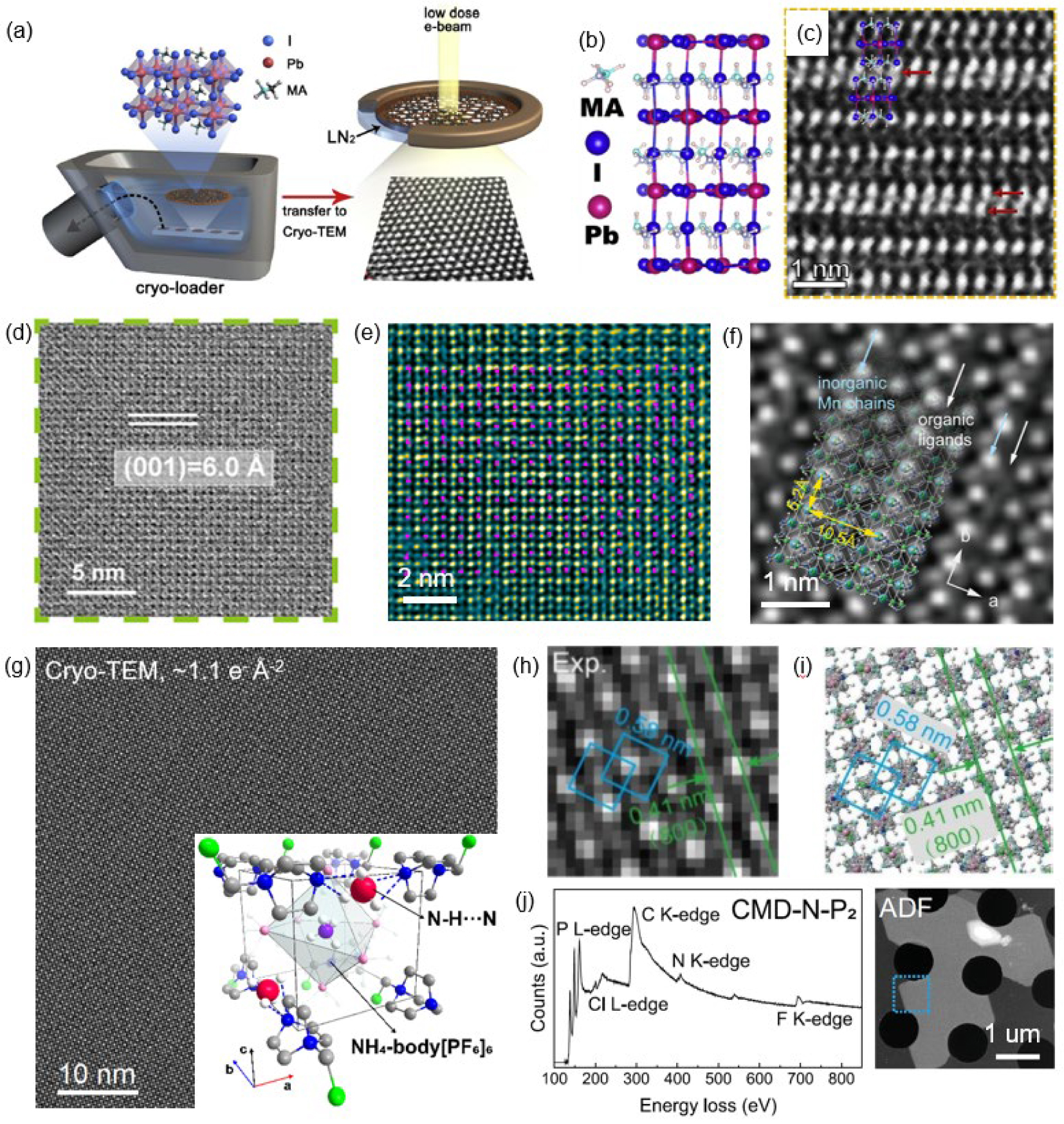
Figure 2. Cryo-TEM characterization of organic–inorganic hybrid and all organic perovskite crystals. (a) Schematics for the high-resolution Cryo-TEM method to preserve air- and beam-sensitive samples under liquid nitrogen protection. The left panel depicts MAPbI3 nanoparticles protected by the Cryo-loader, and the right panel shows Cryo-TEM observation with a low dose electron beam at the cryo-temperature. (b) Atomic model of MAPbI3 view along [3-10] direction. (c) Lattice resolution HRTEM image overlaid with a structural model showing stacking disorder along the (002) surface (electron dose is 94 e−⋅Å−2). Reproduced with permission from Ref. [46]. (d) Atomic-resolution TEM images resolving [PbI6]4− octahedral and MA+ molecule of MAPbBr3 (electron dose is 46 e−⋅Å−2). Reproduced with permission from Ref. [59]. (e) Polarization map based on the quantitative analysis of the MA polarization distribution in the atomic-resolution MAPbI3 image along the [001] zone axis (electron dose, ∼ 5.96 e−⋅Å−2). Reproduced with permission from Ref. [79]. (f) High-resolution lattice fringe image of (FB)2MnCl4 perovskite taken along the [001] zone axis with an overlaid atomic model by single-crystal XRD refinement. The blue and white arrows emphasize the inorganic Mn ion chains with high phase contrast and the organic ligands part with weak phase contrast in between, respectively. The total imaging electron dose is 2.5 e−⋅Å−2. Reproduced with permission from in Ref. [80]. (g) Cryogenic HRTEM image of CMD-N-P2 2D all organic perovskite taken along the [001] direction. The inset displays the pseudo-cubic unit cell of the CL-v phase 2D all organic perovskite. The accumulated electron dose is only 1.1 e−⋅Å−2. (h) A magnified high-resolution image of CMD-N-P2 lattice fringes from a selected area of image (g), and (i) the corresponding atomic model in the [001] axis. (j) The EELS spectrum of CMD-N-P2 exhibits clear onset features of P-L, Cl-L, C-K, N-K and F-K edges, with a representative ADF image shown alongside. Reproduced with permission from Ref. [86].
-
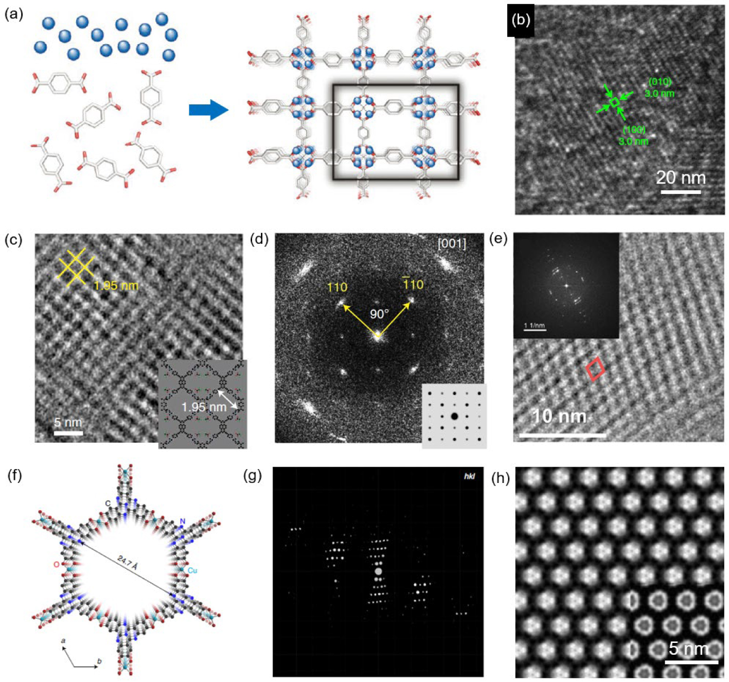
Figure 3. Cryo-TEM characterization of porous materials. (a) Schematic diagram of constructing a molecular skeleton of a porous material from atomic and molecular units. Reproduced with permission from Ref. [90]. (b) High-resolution Cryo-TEM images of homogeneous supramolecular metal-organic framework (SMOF-1). Reproduced with permission from Ref. [95]. (c) Magnified high-resolution lattice fringe image of imidazopyridinium-linked COFs (IP-COF-2) along the [001] direction, which shows interplanar spacings consistent with its atomic structure model (inset). (d) The FFT pattern of the HRTEM image of IP-COF-2, and the inset shows the simulated reciprocal lattice along the imaging zone axis. Reproduced with permission from Ref. [97]. (e) Magnified high-resolution lattice fringe images of pdiCOF-Zn along a tilted c-axis. The inset shows the FFT pattern. Reproduced with permission from Ref. [98]. (f) Single-crystal structure of Cu3HHTT2 along the c direction. (g) 3D reciprocal lattices of a Cu3HHTT2 rod with a maximum resolution of 1.5 Å (hkl corresponds to reciprocal space indices). (h) Averaged high-magnification Cryo-TEM image of a Cu3HHTT2 plate (inset: simulated HRTEM image). Reproduced with permission from Ref. [99].
-
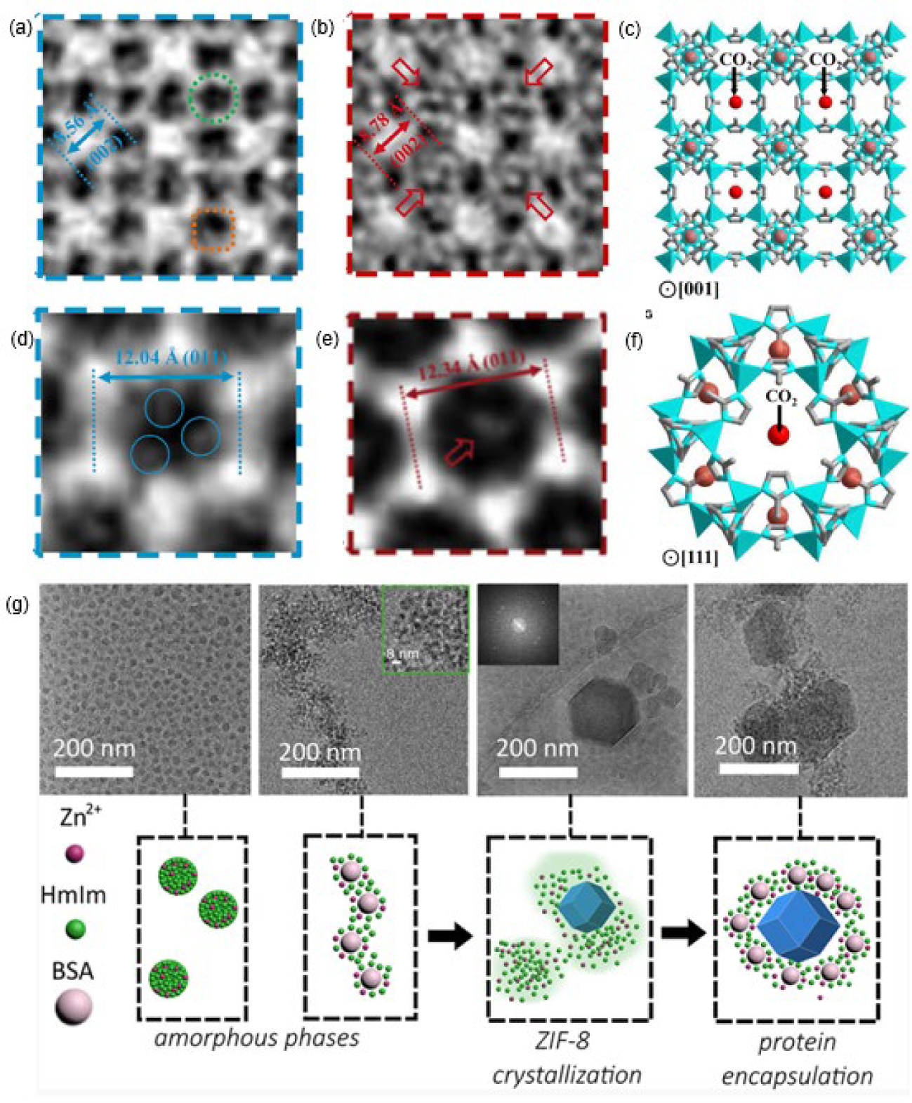
Figure 4. Ex situ and operando Cryo-TEM characterization of porous materials and their dynamic crystallization process. Magnified Cryo-TEM images of (a) vacuum-dried, empty ZIF-8 unit cell and (b) CO2-filled ZIF-8 unit cell, captured at an electron dose of ∼ 7 e−⋅Å−2 along the [111] projection. (c) Simulated ZIF-8 structure with DFT-predicted CO2 binding sites (red spheres) along the [111] projection, consistent with the experimental image in (b). Magnified Cryo-TEM image of (d) vacuum-dried, empty ZIF-8 unit cell and (e) CO2-filled ZIF-8 unit cell, taken at ∼ 7 e−⋅Å−2 along the [001] projection. The green circle indicates the pore cavity at Zn cluster vertices, while the orange square marks the pore cavity at the Zn cluster edges. Density near the center of the unit cell (indicated by red arrows) likely corresponds to CO2 adsorption within ZIF-8. (f) Simulated ZIF-8 structure with DFT-predicted CO2 binding sites along the [001] projection, consistent with image (e). Reproduced with permission from Ref. [54]. (g) Representative Cryo-TEM images and (h) schematic diagrams of nucleation and growth processes of protein-encapsulated ZIF-8 in water. Reproduced with permission from Ref. [103].
-
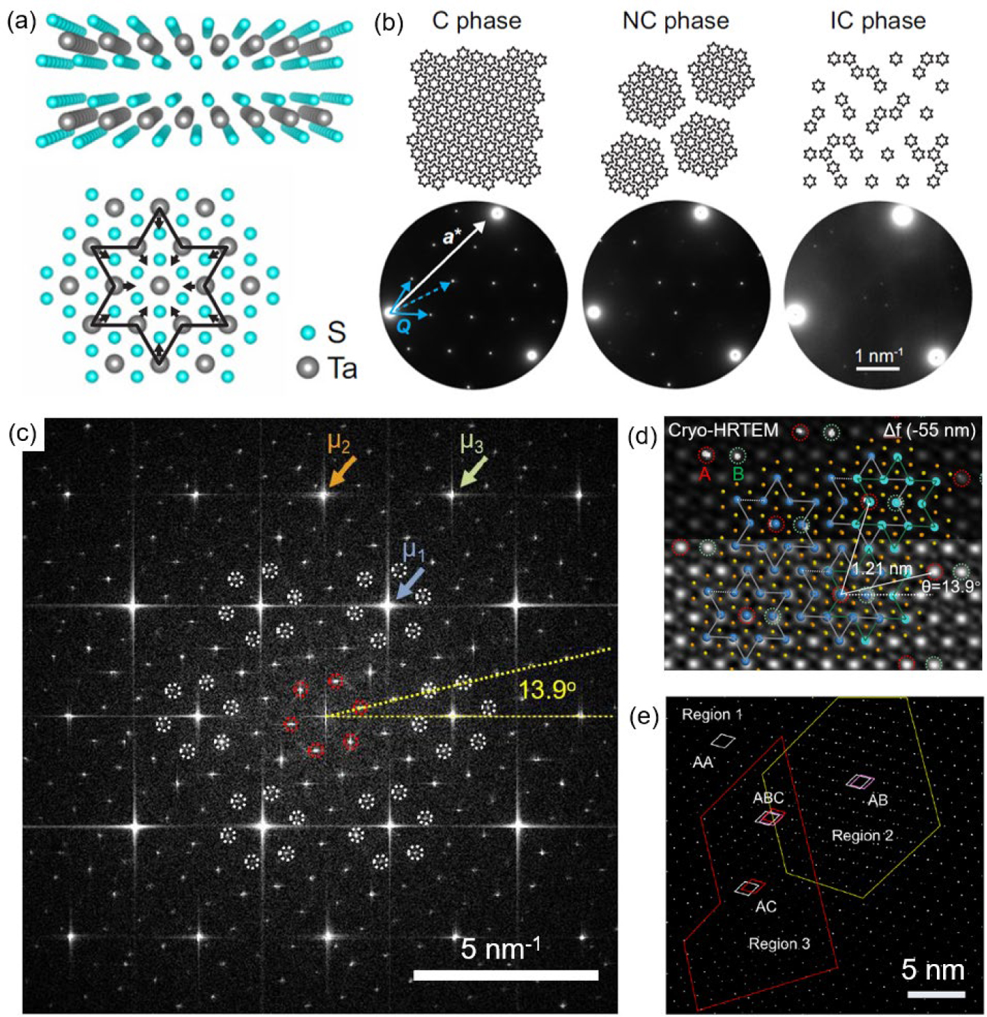
Figure 5. Cryo-TEM characterization of the CDW phase transition and CDW stacking order in 1T-TaS2. (a) Atomic structure of 1T-TaS2 in cross-section and plan-view. The local CDW distortion is shown, forming an SOD structure. (b) Illustration of the C, NC, and IC CDW phases, showing different orderings of the SOD clusters. Associated electron diffraction patterns are exhibited. In the C phase diffraction pattern, ‘a*’ represents the Bragg vector, while the blue solid and dotted lines represent the first-order CDW Q vectors and the second-order CDW vector, respectively. Reproduced with permission from Ref. [114]. (c) Representative FFT patterns of the HRTEM image acquired from an exfoliated 1T-TaS2 flake (thickness 10 nm). μ1, μ2, and μ3 denote the first- to third-order Bragg reflections. Red and white circles mark the first-order PLD reflections and second-order PLD harmonics (scale bar, 5 nm−1), respectively. (d) Cryo-HRTEM image of 1T-TaS2 acquired at a defocus value of −55 nm. TEM phase intensity analysis reveals an AB stacking configuration for its SOD superstructure, indicated by overlapping atomic structural patterns. (e) 3D arrangement of SODs obtained by Fourier bandpass filtering based on PLD-related wave vectors. Local AB and AC domains of SOD stacking, highlighted by yellow and red lines, respectively, coexist with AA stacking. Reproduced with permission from Ref. [119].
-
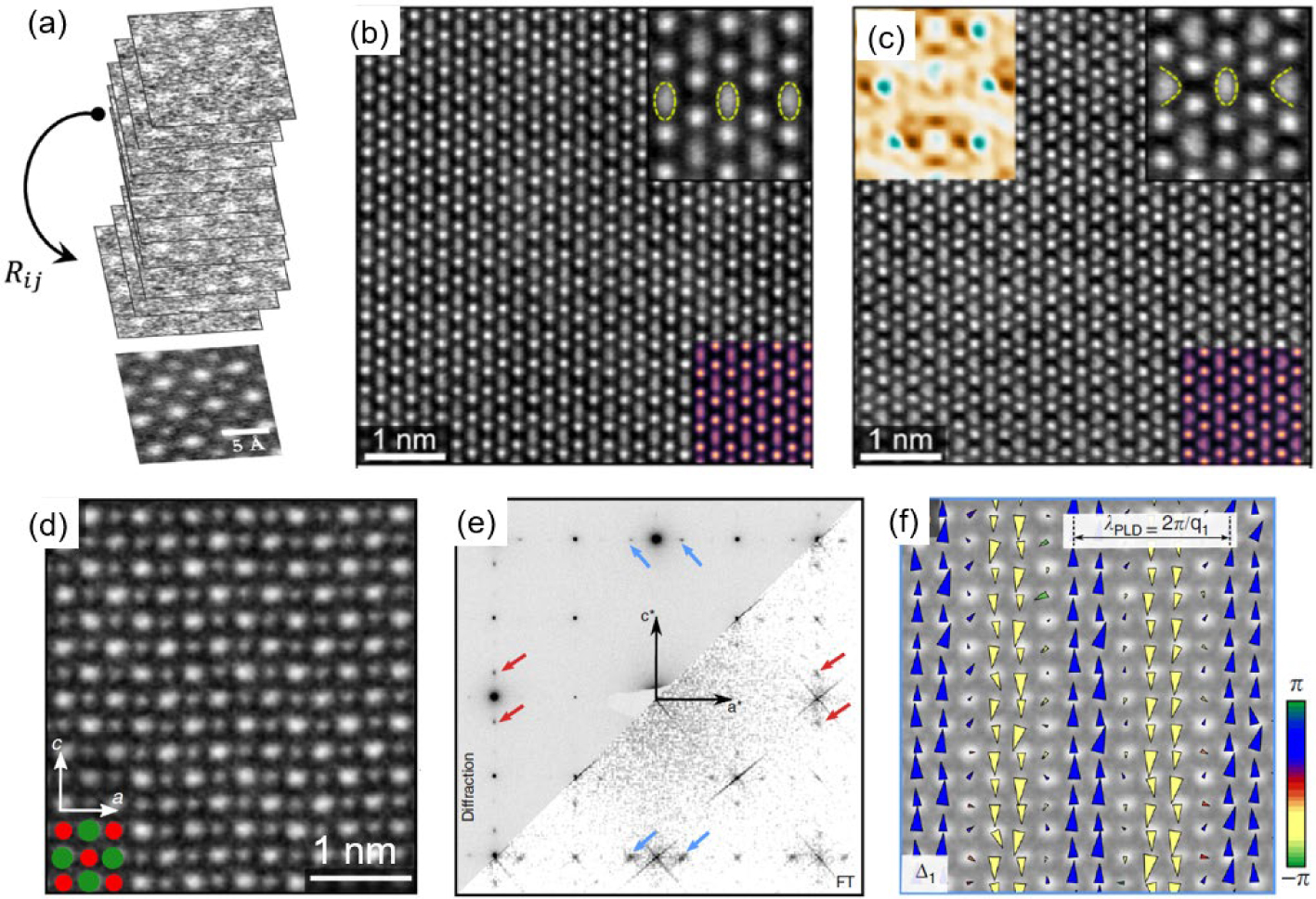
Figure 6. Cryo-TEM/STEM characterization of charge order concomitant PLDs. (a) All possible image pairs in a stack of fast Cryo-STEM acquisitions are cross-correlated to determine relative shifts. Reproduced with permission from Ref. [120]. (b) and (c) STEM images of 1T′-TaTe2 at (b) 293 K and (c) ∼ 95 K. In the magnified views of the images, no distortion is observed at 293 K, whereas distortion becomes apparent at 95 K. Reproduced with permission from Ref. [121]. (d) HAADF-STEM image of BSCMO at 95 K (scale bar = 1 nm). (e) Electron diffraction over a 1 μm selected area and the Fourier transform of a 30 nm field of view STEM image of BSCMO along the b*-axis. Satellite peaks corresponding to two transverse and displacive modulations with perpendicular wavevectors q1 ≈ 1/(3a*) and q2 ≈ 1/(3c*) are indicated by blue and red arrows, respectively. (f) Mapping of picometer-scale PLDs at each atomic lattice site in response to a single modulation along the c axis. Triangles represent displacements, with their area scaling linearly with displacement amplitude. Color represents the angle of the polarization vector. Reproduced with permission from Ref. [122].
-
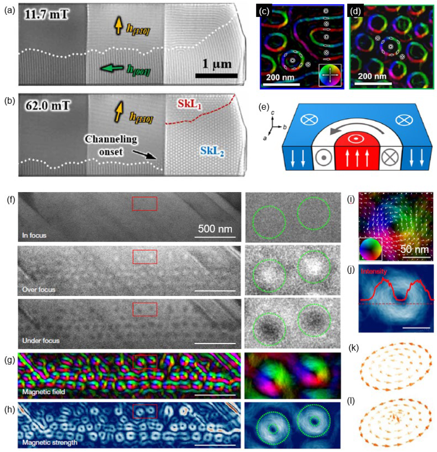
Figure 7. Low-temperature LTEM characterization of topological spin textures. [(a) and (b)] Helical-to-skyrmion phase transition in Te-doped CSO observed by Lorentz microscopy at 25 K under external magnetic fields (H) of 11.7 mT and 62 mT applied along the [110] direction. Reproduced with permission from Ref. [124]. [(c) and (d)] Magnetization maps obtained from regions with tripes and skyrmionic bubbles, respectively, using transport-of-intensity equation (TIE) analysis. (e) Schematic representation of the skyrmionic bubble spin texture. Reproduced with permission from Ref. [125]. (f) Fresnel mode LTEM micrographs of the zero-field state (300 K) acquired at the [001] zone axis with varying defocus values (Δ f = ± 1.08 mm). (g) and (h) Real-space magnetization textures and corresponding magnetic field strength obtained by QPt software based on the TIE analysis. Scale bars in (f)–(h) are 500 nm. The right panel shows enlarged images of the red-boxed regions. (i) and (j) High-magnification (scale bar, 50nm) magnetization texture (i) and corresponding magnetic strength (j). Arrows and the color scale indicate the in-plane magnetization direction and magnitude. (k) and (l) Schematic diagrams of the two possible topological magnetic structures deduced from the LTEM results. Reproduced with permission from Ref. [126].
Figure
7 ,Table
0 个