-
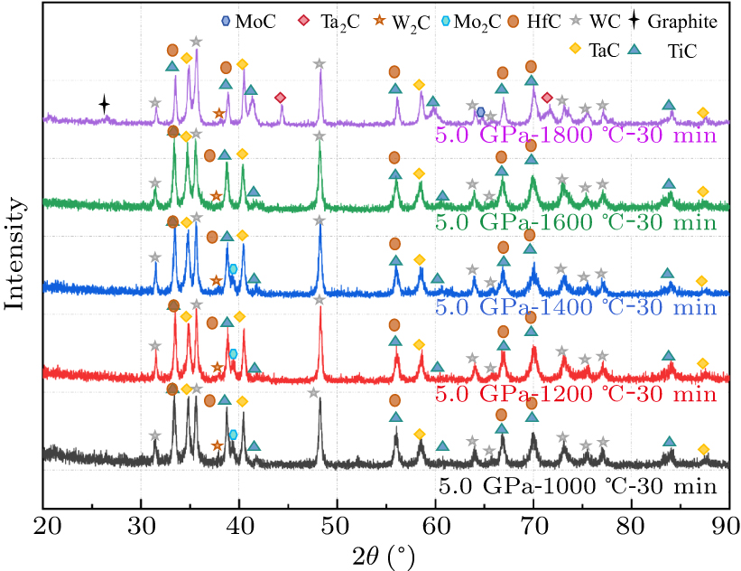
Figure 1. XRD patterns of five samples recovered from different conditions indicated by T (in °C) pairs.
-
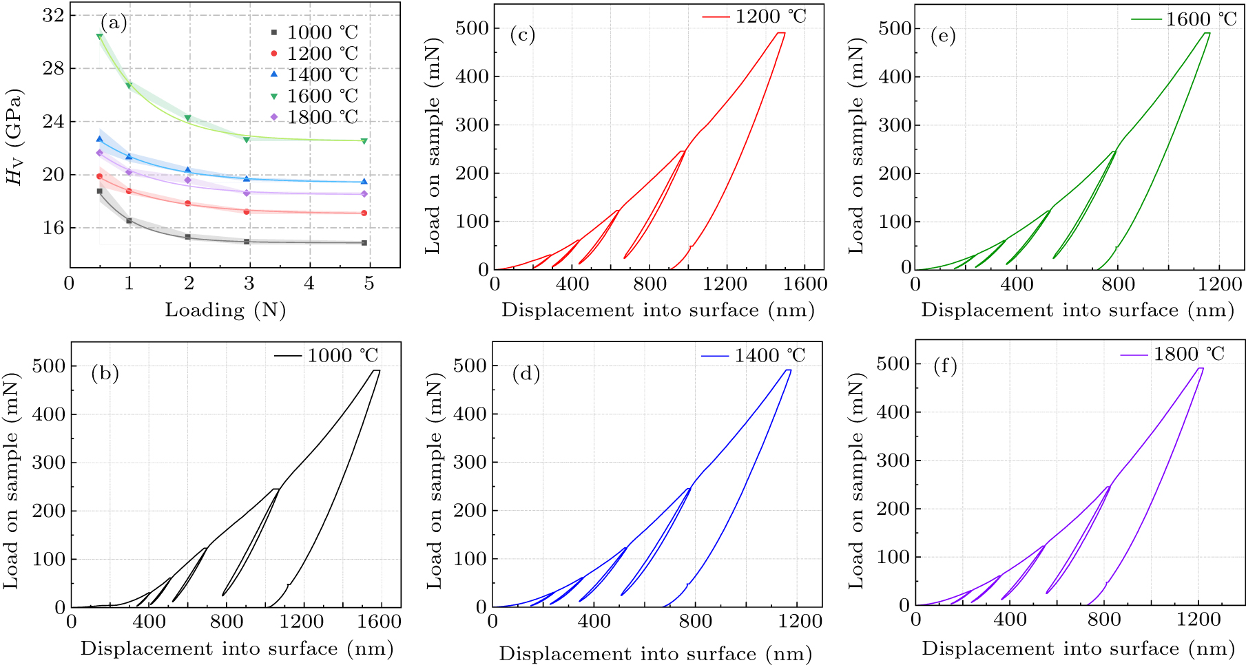
Figure 2. Mechanical test results of five samples recovered from different conditions. (a) Vickers hardness test results of five synthesized samples recovered from different conditions indicated by T (in °C) pairs. (b)–(f) Loading and unloading curves of indentation tests for five synthesis samples recovered from different conditions indicated by T (in °C) pairs.
-
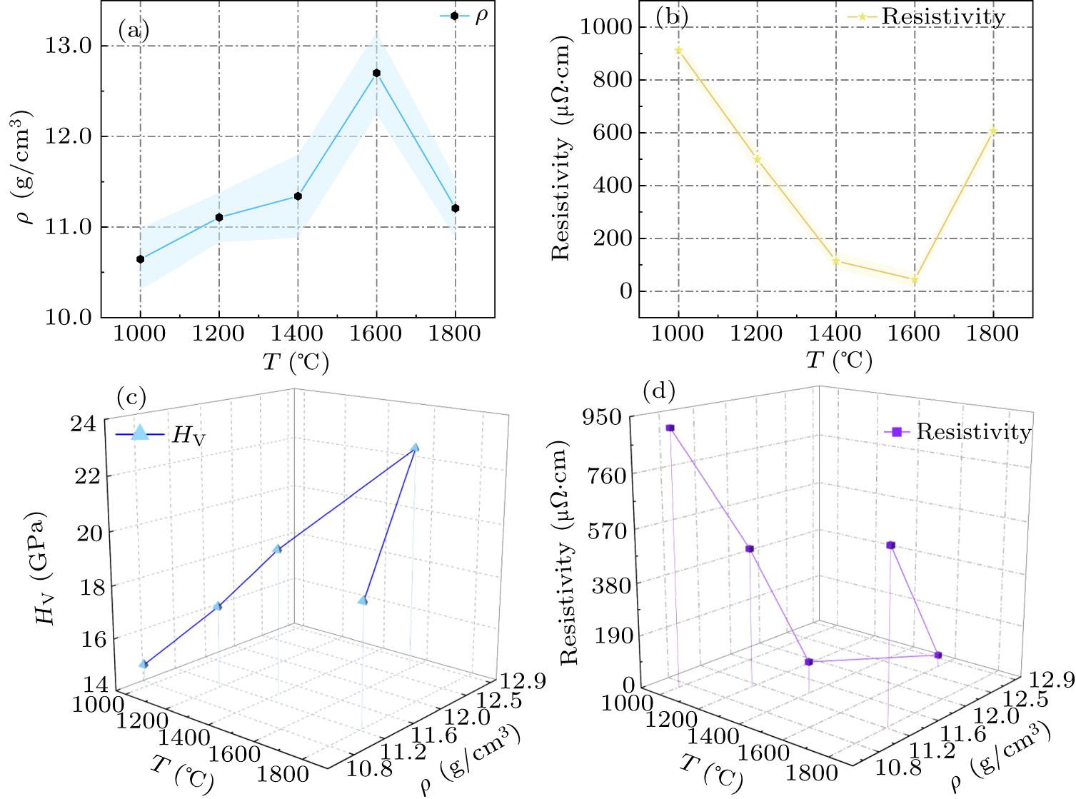
Figure 3. Other physical properties of five samples recovered from different conditions indicated by T (in °C) pairs. (a) Density results of five synthesized samples recovered from different conditions indicated by T (in °C) pairs. (b) Resistivity results of five synthesized samples recovered from different conditions indicated by T (in °C) pairs. (c) Trend of the relationship between Vickers hardness, density, and temperature. (d) Trend of the relationship between resistivity, density, and temperature.
-
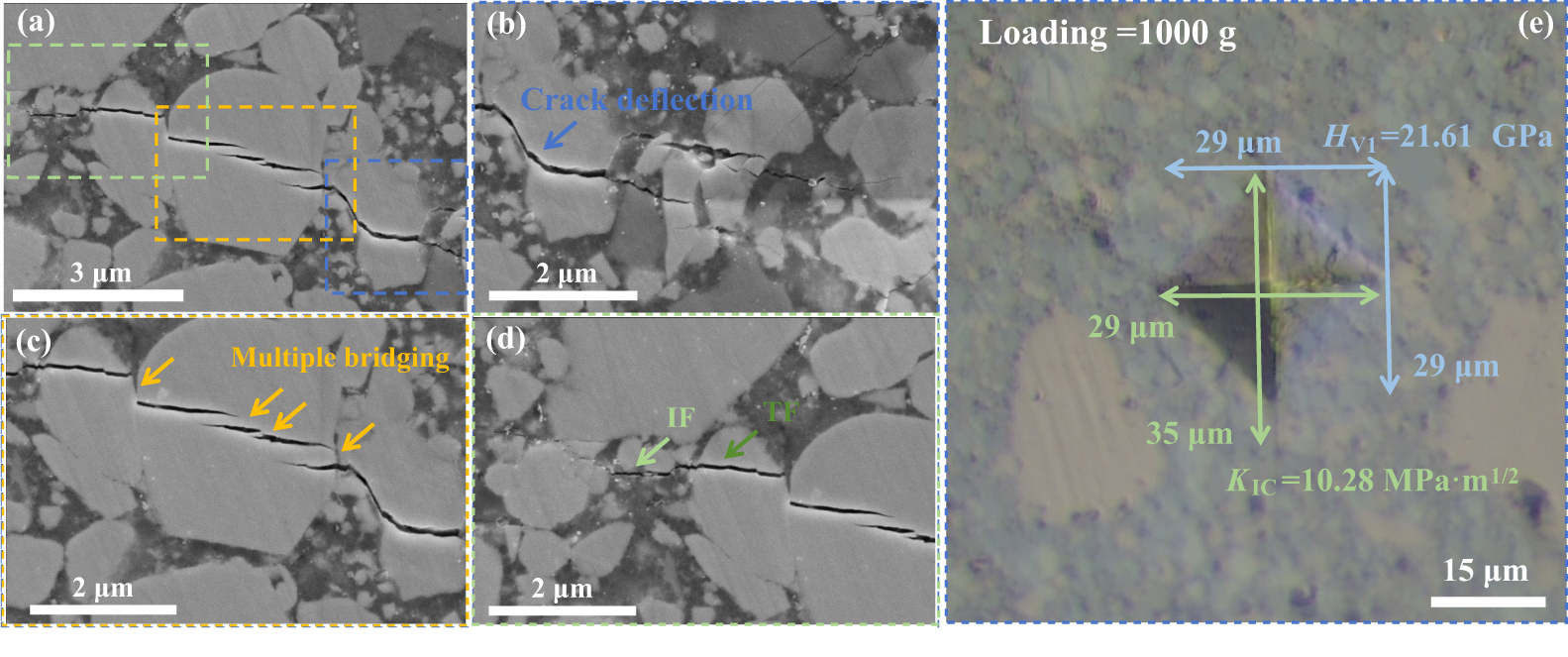
Figure 4. Typical toughening mechanisms in the HEC-4. (a) SEM image of the crack propagating in the HEC-4. The blue dashed area shows crack deflection. The yellow dashed area shows multiple bridging. The green dashed area shows transgranular fracture (TF) mixed with intergranular fracture (IF). (b) SEM image of microstructure of crack deflection, corresponding to the blue-boxed area in (a). (c) SEM image of multiple bridging, corresponding to the yellow-boxed area in (a). (d) SEM image of TF mixed with IF, corresponding to the green-boxed area in (a). (e) Vicker indentation with a load of 9.8 N.
-
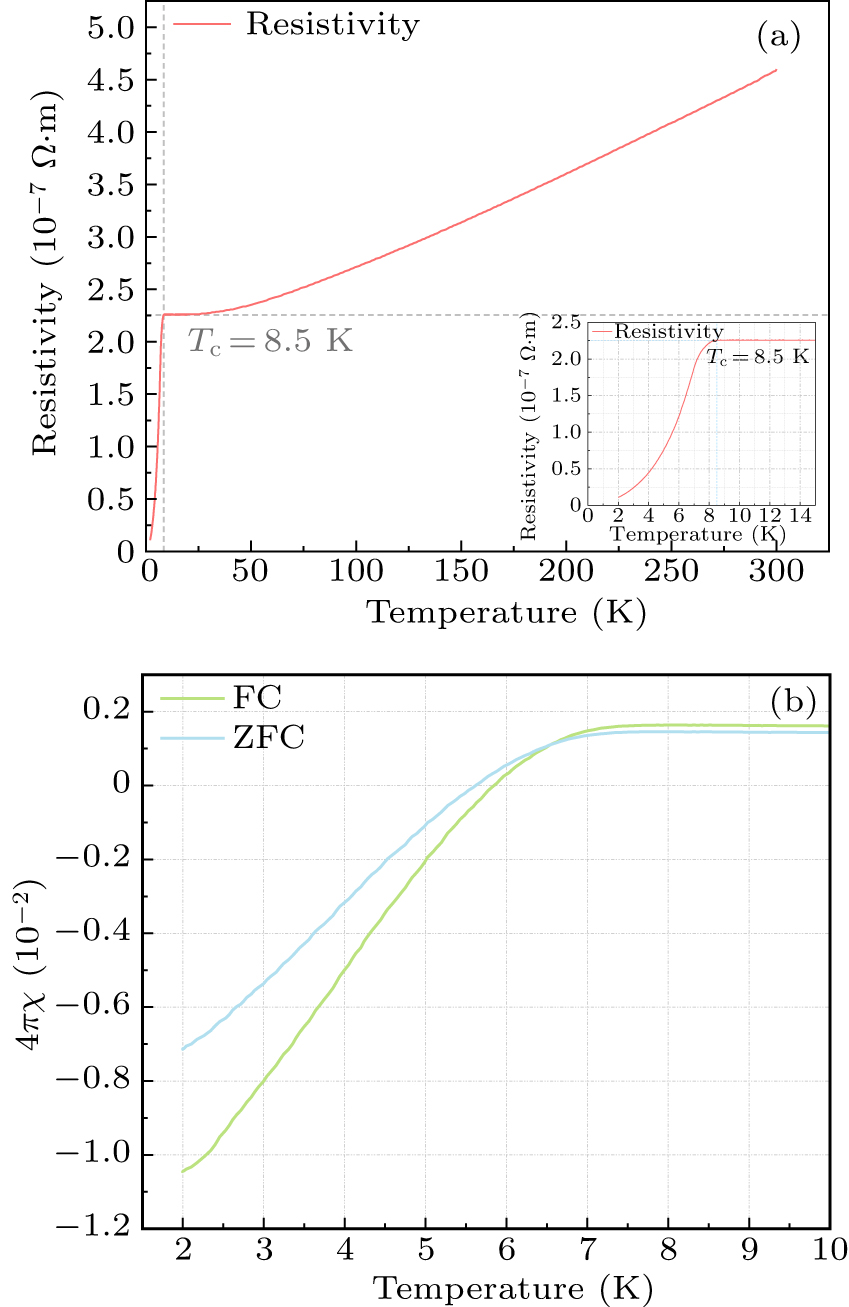
Figure 5. The testing results of the physical property measurement system (PPMS). (a) The temperature dependence of resistivity (ρ–T) curve of HEC-4. The inset shows the localized magnified image near Tc. (b) The temperature dependence of field-cooling magnetization (green) and zero-field cooling magnetization (blue) curves of HEC-4.
-
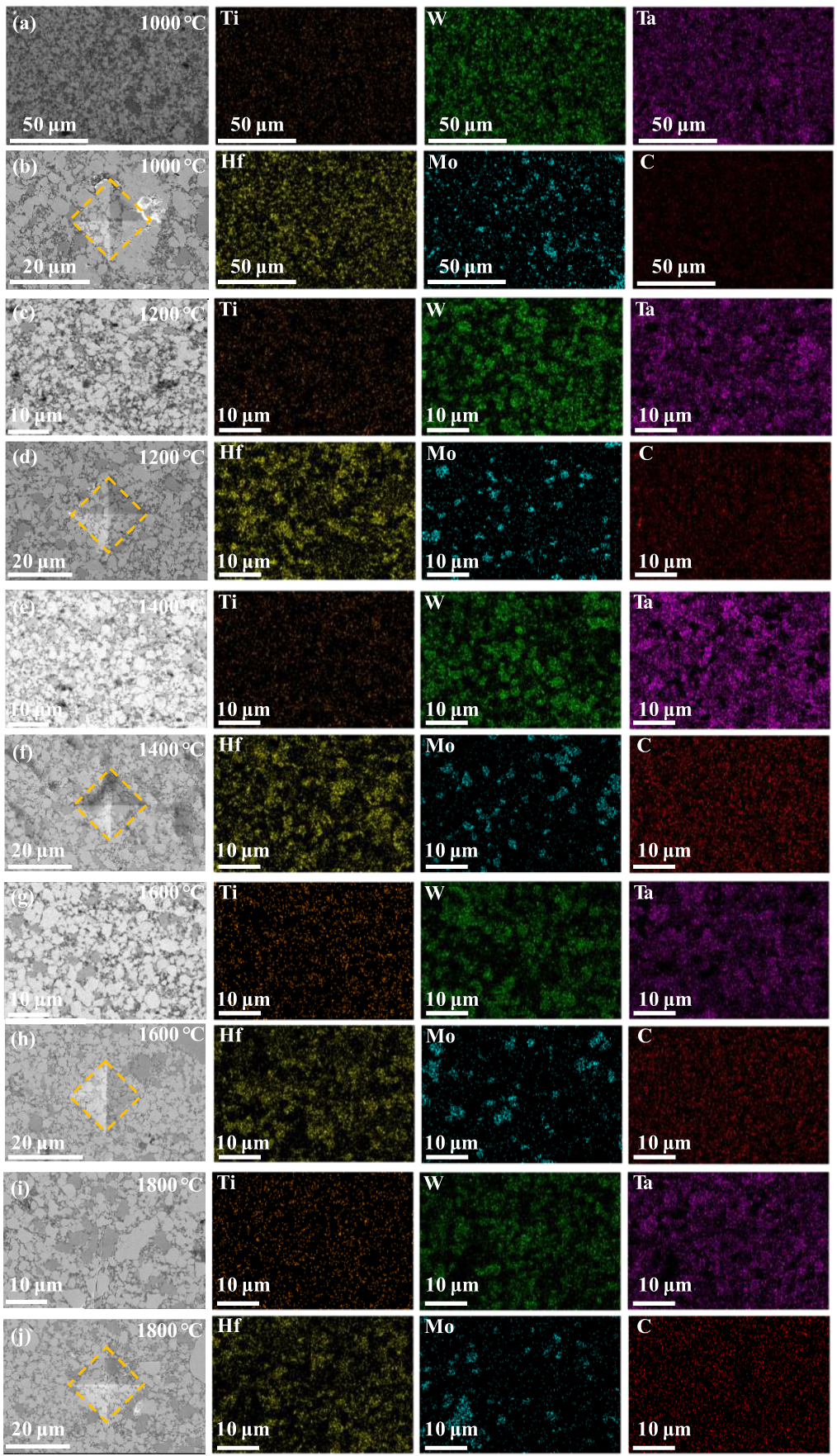
Figure 6. SEM images of HEC-1, HEC-2, HEC-3, HEC-4 and HEC-5. (a), (c), (e), (g), (i) SEM images and corresponding EDS mapping showing the elements distribution in the polished surface of sample HEC-1, HEC-2, HEC-3, HEC-4 and HEC-5 after sintering at different temperature for 30 min; EDS mapping analysis: C element (red), Ti element (orange), Hf element (yellow), Ta element (purple), W element (green), and Mo element (blue). (b), (d), (f), (h), (j) SEM indentation images of sample HEC-1, HEC-2, HEC-3, HEC-4 and HEC-5 after sintering at different temperature for 30 min.
Figure
6 ,Table
2 个