-
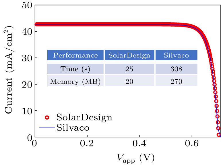
Figure 1. The J–V characteristics of the TOPCon silicon solar cell. The comparisons of computer time and memory cost between SolarDesign platform and Silvaco are also presented. 1000 sampling points are adopted for the J–V characteristics.
-
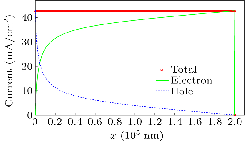
Figure 2. Classical total, electron, and hole currents of the TOPCon silicon solar cell under the short-circuit condition, where 1 nm silica layer is used for electron current tunneling and surface recombination reduction.
-
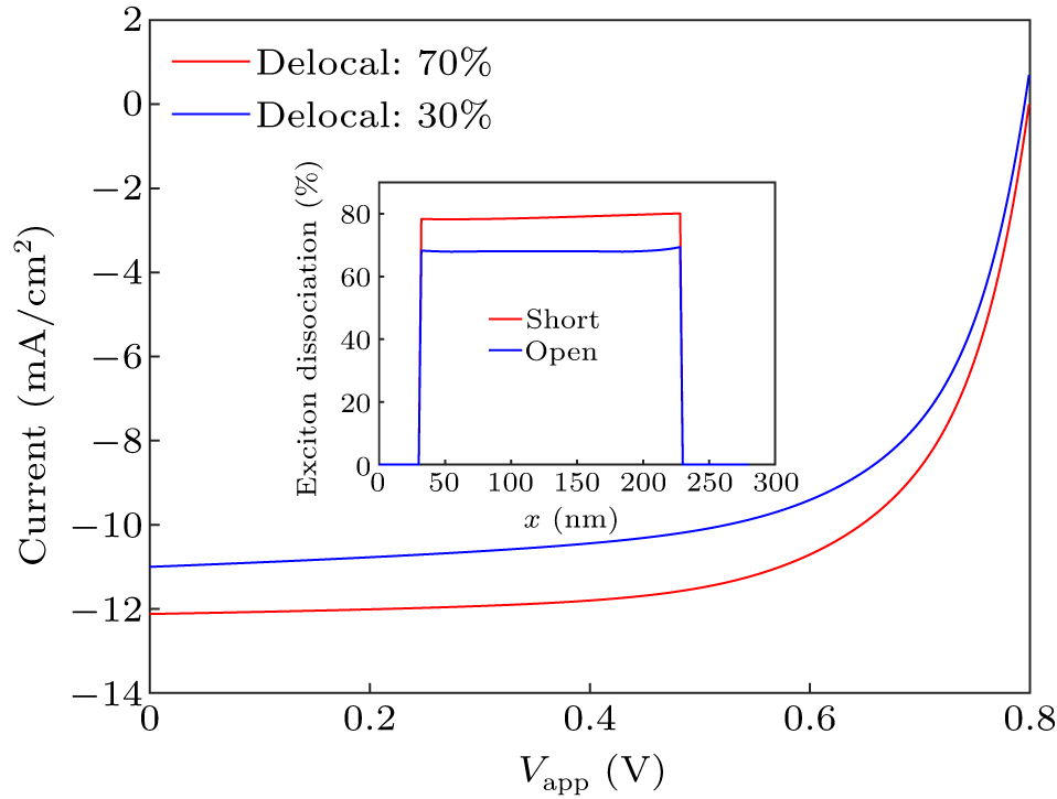
Figure 3. The J–V characteristics of the organic solar cell. “Delocal” denotes the delocalization ratio of exciton. The inset shows the exciton dissociation probabilities under the short-circuit and open-circuit conditions.
-
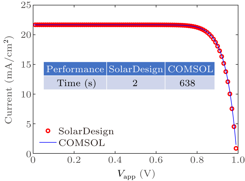
Figure 4. The J–V characteristics of the perovskite solar cell. The comparison of computer time between SolarDesign platform and COMSOL is also presented. 1000 sampling points are adopted for the J–V characteristics.
-
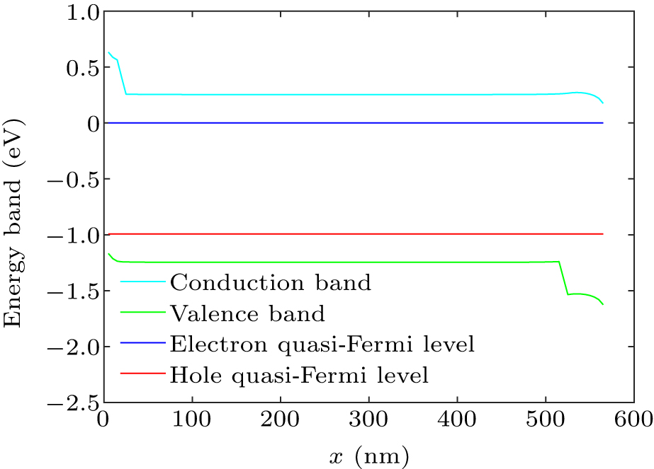
Figure 5. Energy band diagram of the perovskite solar cell under the open-circuit condition.
-
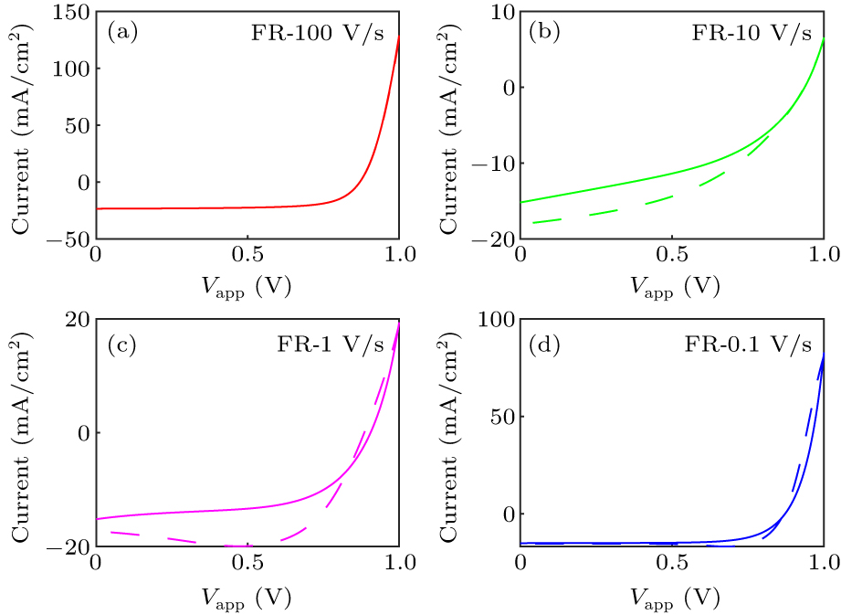
Figure 6. The J–V hysteresis of the perovskite solar cell with different voltage scanning rates (V/s). The forward–reverse (FR) scanning mode is adopted. Solid and dashed lines denote forward and reverse scans, respectively.
-
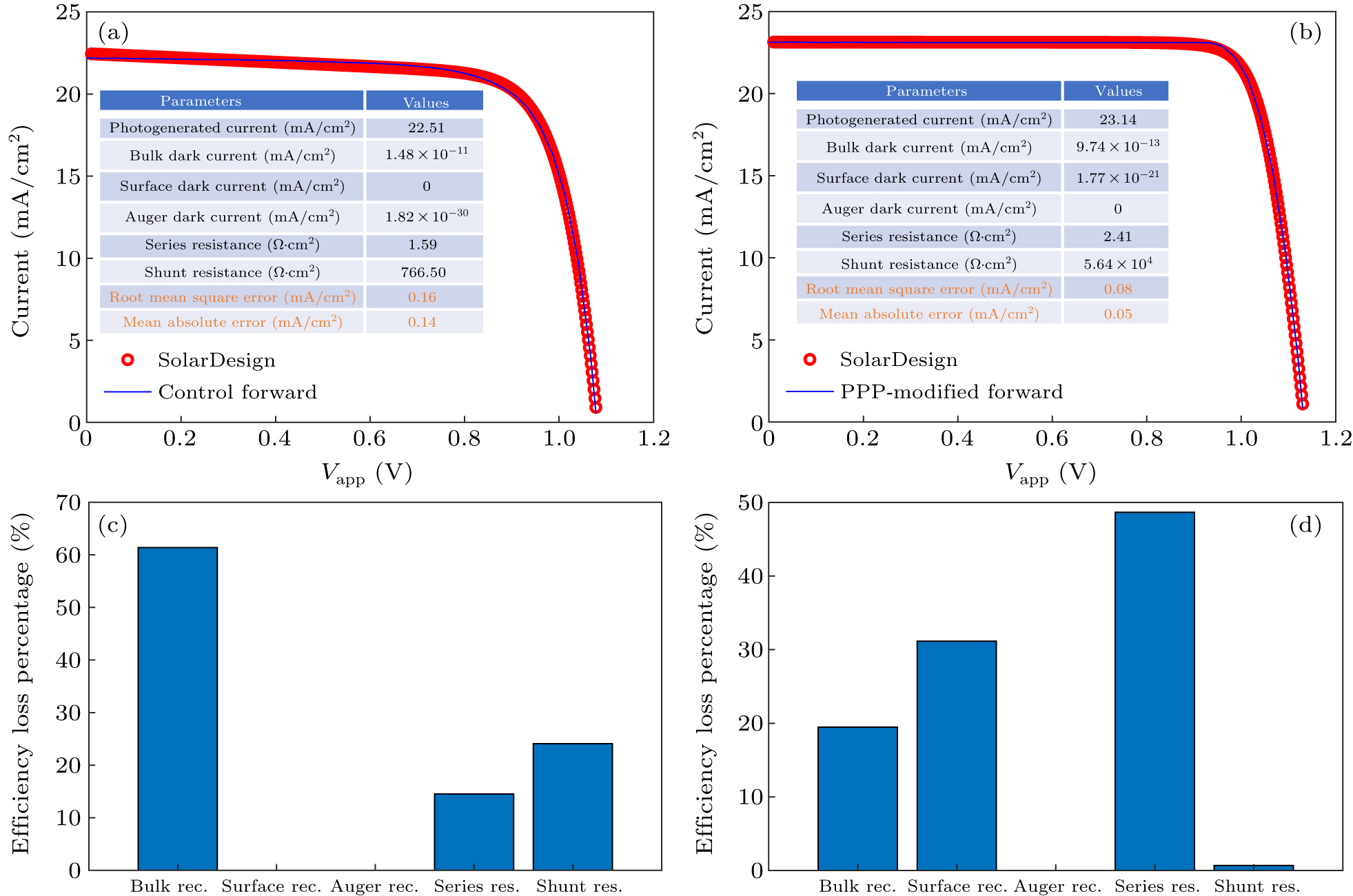
Figure 7. The J–V characteristics and efficiency losses of perovskite solar cells. (a) and (b) The J–V characteristics of the control and polymer incorporated (PPP-modified) cells, respectively; the insets show the circuit parameters and fitting errors. (c) and (d) The quantified efficiency losses of the control and polymer incorporated cells, respectively.
Figure
7 ,Table
3 个