
 首页
首页 登录
登录 注册
注册


-
Since the discovery of graphene,[1] two-dimensional (2D) materials, especially in the ultra-thin-film form, have aroused researchers’ enthusiasm and demonstrated a variety of remarkable physical properties including nontrivial topology,[2–4] superconductivity,[5,6] ferroelectrics,[7,8] valleytronics,[9] etc. Molecular beam epitaxy (MBE) is one of the key ways to obtain high-quality thin films, including a wide range of ultra-thin films of elementary substances, such as bismuth,[10,11] stanene,[12] blue phosphorus,[13] etc. Tellurium (Te), as one of the group III–VIA elements, has undergone extensive studies in the applications of infrared photosensors[14] and field-effect transistors.[15,16] The high-quality Te nanosheets were synthesized by using chemical vapor deposition[14] or a substrate-free solution process.[15] They exhibited ultrahigh hole mobility, high blackbody responsivity, and air-stable performance at room temperature. Nonetheless, the study of ultra-thin Te film is rare, especially for the few-monolayer case.
At ambient conditions, the bulk Te is one kind of narrow bandgap semiconductor (∼ 0.34 eV), formed of parallel-arranged helical Te chains of atoms and belonging to the trigonal lattice. The interchain atoms are connected via van-der-Waals interactions in contrast to the intrachain strong covalent bonds. The helical chains of Te form a hexagonal network in the plane perpendicular to the chains. The helicities of Te chains are distinguished by space groups P3121 and P3221. Bulk Te may undergo a topological band inversion under shear (hydrostatic or uniaxial) strain.[17] In the thin-film case, recent theories and experiments show that Te has three phases: α-Te, γ-Te, and β-Te. Here α-Te and γ-Te are formed owing to the multivalency of Te.[18] When the thickness of bulk Te is reduced to a few layers, the bulk phase automatically transforms into the β-Te phase, which is the most stable structure among these three phases. Furthermore, the theoretical calculation has predicted a new phase, the square-Te, which is a 2D topological insulator that opens an inversion band gap of nearly 170 meV.[19] A substrate with suitable lattice parameters is a prerequisite for the MBE growth of desired phase. To realize the possible non-trivial phase of Te, SrTiO3 (STO) (001) is the promising substrate because of its small lattice mismatch (<1%) with square-phase Te.[20] Currently, some experiments have been successful in producing Te films. Nonetheless, among the various reports on the MBE growth of β-Te films on graphene, HOPG, and NbSe2 substrates,[21–24] there is no attempt on the substrates with square lattice. In addition, up to now, ultra-thin films of Te with full-coverage and controllable thickness have not been achieved.
In our work, ultra-thin Te films are successfully grown on STO (001) substrates. We adopt a low-temperature (LT, liquid nitrogen temperature) deposition and fast-annealing (FA) method to circumvent the thermodynamic limitations in the Te/STO system that lead to the Volmer–Weber (VW) growth mode of Te, and make it possible to achieve the ultra-thin and flat films with nearly complete coverages. Different layers of Te films can thus be obtained by changing the growth time. Te films undergo a critical behavior at the thickness of 3 monolayer (ML). Below 3 ML, Te films basically show amorphous phases. Above 3 ML, Te films show complete coverage and thickness-controllable morphology. The films are found to be β-Te instead of the desired square phase that matches better with the STO (001) substrate. Meanwhile, scanning tunneling spectra (STS) of ultra-thin Te films above 3 ML are acquired and show that ultra-thin Te films have much larger band gaps compared with those reported.[21,22] For example, the 3-ML Te film on STO (001) has a gap of ∼ 1.4 eV, which is nearly twice of that grown on graphene.
Our experiments were performed in a combined MBE (base pressure <2 × 10⁻¹⁰ Torr) and low-temperature scanning tunneling microscopy (STM) system (Unisoku 1300). The Nb-doped STO (001) (Nb:0.7 wt.%, Hefei KMT) were treated by the standard cleaning procedure including dipping in buffered oxide etchant (BOE, NH4F/HF 7:1) for 35 s.[25,26] In the MBE chamber, the substrates were first degassed and then annealed at 930 °C for 2.5 hours to get the (2 × 2) reconstruction. Ultra-high-purity tellurium (99.9999%) was evaporated from a standard Knudsen cell at a flux rate of ∼ 1 Å/min. After growth and recording the RHEED pattern, the sample was transferred into the STM system at 5.4 K. STS were acquired using a standard lock-in technique with a modulation voltage of 10 mV and at a frequency of 987.5 Hz at 5.4 K. The STM topographic images and spectra were processed with WSXM software.
To obtain high-quality films, we use the (2 × 2) reconstructed surface of the STO (001) substrate, which is TiO2-terminated and can be obtained by the process described above. The presence of TiO2 (2 × 2) reconstructed surface can be confirmed by the atomically flat morphology as shown in the STM image of Fig. 1(a) as well as the sharp (2 × 2) RHEED pattern (insert). In a smaller scale, the high-resolution STM image and fast Fourier transform pattern (FFT) are shown in Fig. 1(b), similar to the results in the literature.[27] Figure 1(f) (upper one) shows the topographic profile along the dark blue line in Fig. 1(a) and gives the step-height of STO (001), h = 0.39 ± 0.01 nm. The surface roughness of the reconstructed substrate is ∼ 50 pm (peak to peak). We thus obtain an atomically flat substrate to allow for the growth of high-quality ultra-thin films.
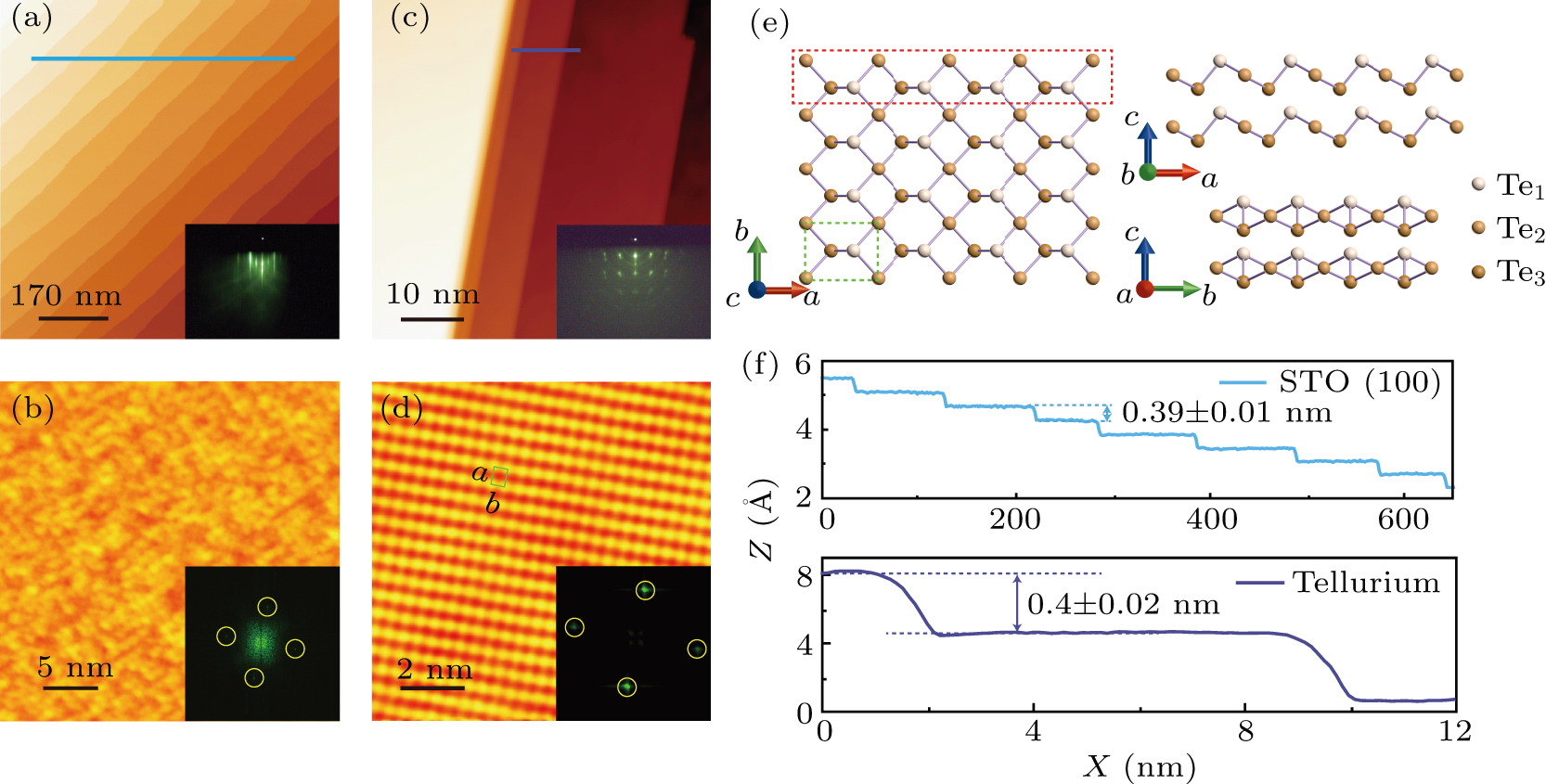
First, we grow Te films by using the normal procedure (high temperature growth, HT). During the growth, the substrate is kept at 80 °C, which is slightly above the activation temperature (Td, as described later) for the diffusion of Te on the STO (001) (2 × 2) substrate. The growth follows the typical VW island growth mode without the formation of the wetting layer. The circle- and dot-like shapes in the RHEED patterns (insert of Fig. 1(b)) also confirm the morphology of the film to be made of clusters and islands. Figure 1(c) is the topographic image of part of an island. The sectional profile along the dark blue line is shown in Fig. 1(f), indicating a step-height h′ = 0.40 ± 0.02 nm. The in-plane lattice constants a and b are measured to be 0.547 nm and 0.427 nm as shown in the atomic resolved image (Fig. 1(d)) and the corresponding FFT image (insert). The rectangular lattice and the lattice constants are consistent with relevant reports on β-Te.[18,28] Thus, the film obtained by the HT growth is the β-Te phase, which is the most stable one when the bulk Te is reduced into the ultra-thin film form.[18] As the thickness of bulk Te decreases, the interactions between the Te helical chains get stronger, resulting in additional covalent bonds between the helical chains that are van-der-Waals linked in the bulk form. The structure of β-Te is shown in the ball-and-stick model in Fig. 1(e). The red dashed box represents Te′s helical chain. The green dashed box marks the unit cell of β-Te. The monolayer tellurium is formed by the successive Te1, Te2, and Te3 layers from the surface. The films are grown in the c direction. The unit cell formed by a and b is rectangular which is consistent with the experimental data.
This kind of VW growth mode is due to the condition of γTe + γi – γS > 0, where γTe, γS and γi are the surface energies of Te films and the substrate, and the interface energy, respectively. In addition, it seems that the activation temperature for the diffusion of Te across the Te-steps is lower than that for the diffusion of Te on the substrate. That is, when grown above Td, there only appear 3D islands of Te. Thus, there seems no kinetic barriers for Te atoms to reach the thermodynamic equilibriums on the substrate.
Here, by the LT/FA method we can circumvent the thermodynamic limitations mentioned above by driving the epitaxial dynamics to the extreme condition as described below. First, Te atoms are deposited onto the substrate at 80 K. Second, the sample is then annealed up to the temperature near Td. We find that Te ultra-thin films with a nearly completed coverage can form on the substrate above 3 ML, below which the film stays amorphous.
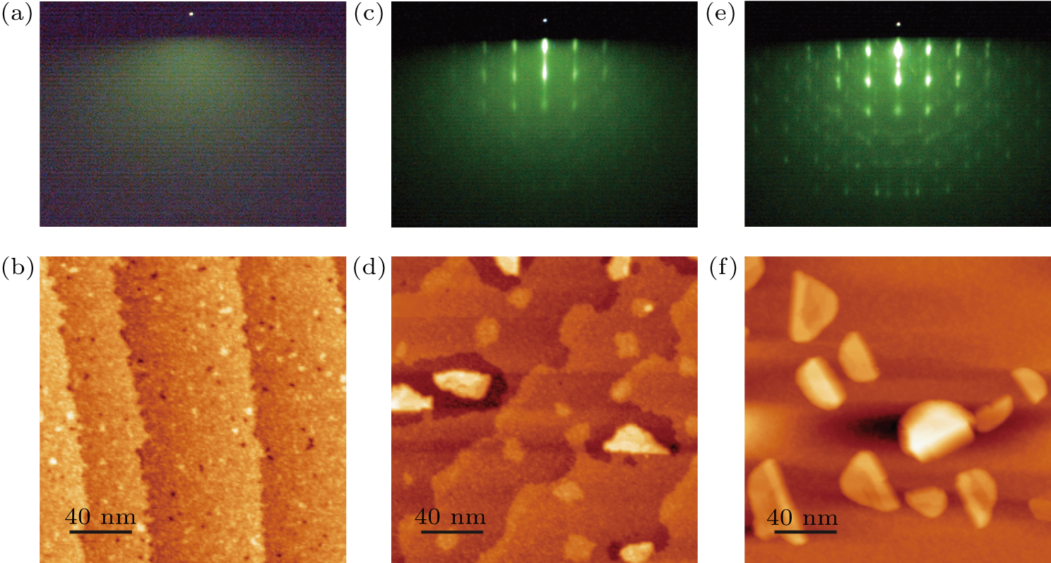
Figure 2 shows the STM images and RHEED patterns for Te films (2 ML) after LT deposition, after FA around Td, and after FA to 80 °C (above Td), respectively. We see that the as-grown film is amorphous and stays amorphous after annealed to some critical temperature at which the RHEED pattern starts to change. This critical temperature is denoted as Td indicating the activation temperature for the diffusion of Te atoms on the substrate. After annealed above Td, only 3D islands form on the substrate. The RHEED patterns for the films at these growth steps are consistent with their morphologies indicated by the corresponding STM images. After the first step, the film is non-crystalline and there is no feature in the RHEED pattern. The STM image in Fig. 2(b) also confirms that the LT-grown Te film on STO (001) substrates is in the amorphous state and does not have enough kinetic energy to diffuse and react on the substrate surface. Compared to the HT growth, the LT growth allows Te atoms to be uniformly spread flat on the substrate, providing a necessary condition for the successful growth of nearly fully covered 2D Te films described later. After the third step, the dotted RHEED pattern indicates that the film is dominated by 3D islands. The growth behavior for 1 ML is similar. Thus, below 3 ML Te atoms only crystallize into 3D islands instead of flat films.
Above 3 ML, things become drastically different. Figures 3(a) and 3(b) are the RHEED pattern and the STM image for the film (3 ML) after the LT/FA process around Td. As shown in Fig. 3(b), except for small holes corresponding to the uncovered substrate, the STM image shows that the film has a nearly complete coverage with a uniform thickness of ∼ 1.35 nm. The clear and sharp streak-lines in the RHEED pattern also indicate the good crystallinity of the film. In Fig. 3(c). the atomically resolved STM image as well as the FFT results shows that the film is in the rectangular β-Te phase and that the in-plane lattice constants are 0.544 nm and 0.433 nm, which are similar to the results of HT growth. Thus, the LT-grown Te film also tends to be in the β-Te phase.
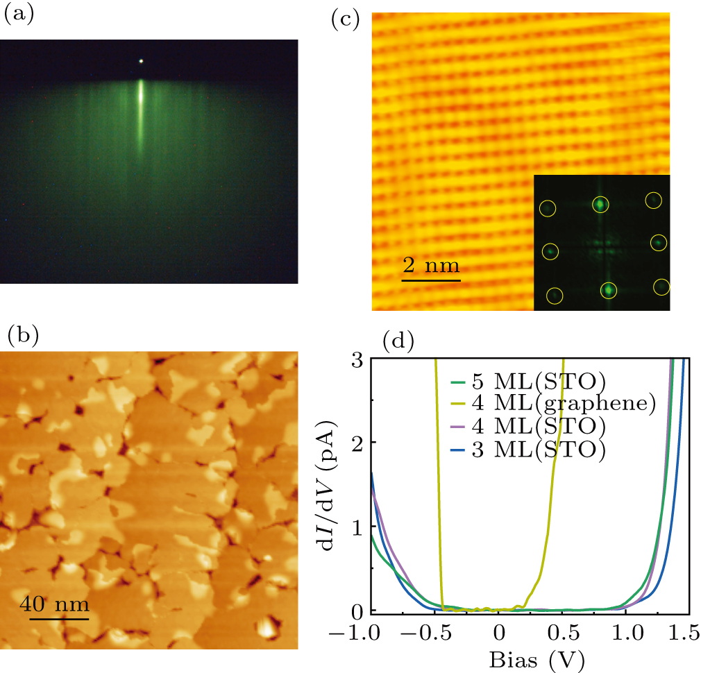
The growth behaviors for films between 3 ML and 7 ML are similar, the resulting Te films exhibit nearly complete coverages and are composed of large domains. This property provides an ideal platform for exploring the remarkable electronic structures of the ultra-thin β-Te films. Figure 3(d) shows the STS obtained on films (from 3 ML to 5 ML) prepared by the LT/FA approach on STO (001) as well as that of the 4-ML film grown on the graphene substrate. We see that the forbidden gap for the 3-ML film on STO (001) is about 1.4 eV, which is unexpectedly large and is almost twice that for the film on graphene. The gap decreases with the increasing thickness similar to the films on graphene.[21] The unusually large gaps may be resulted from the possible strain presented in the films on the STO (001) substrate.
To explain the critical behavior in the occurrence of the flat and ultra-thin films, we propose a possible scenario as described below. Here we have related key thermodynamic parameters γTe, γS, γi, Ef, which are the surface energies of the Te film and the substrate, the interface energy per unit area, and the formation energy of the Te film, respectively. As shown schematically in Fig. 4(a), in the normal HT growth, to determine which type of growth mode that the epitaxial process follows, we examine thermodynamically the possibility for the first-wetting-layer formation. The HT growth follows the VW growth mode without the wetting-layer formation, indicating that the condition II is not energetically favorable compared with the condition III. This means γTe + γi – γS > 0, that is, the surface energy of the Te film plus the interface energy is larger than that of the substrate. This situation prohibits the formation of the wetting layer. To determine the possibility of the formation of flat films, we compare conditions I and II. Here things are different compared with the HT growth mode. The Te atoms deposited on the substrate do not diffuse and form a uniform amorphous film, which crystallizes into the β-phase film after annealing with an energy reduction of Ef (the formation energy). Thus, in the LT/FA growth mode, there appears an additional thermodynamic variable Ef(n) in the above equation that determines the growth mode. Here Ef(n) is thickness dependent and increases with the amount of Te atoms deposited (n ML). Now the expression γTe + γi – Ef (n) – γS is considered for the possibility of turning condition I into condition II. Our experimental results imply that the above expression is positive for n < 3 and becomes negative for n ≥ 3. This explains quite well the critical behavior that flat films only form for n ≥ 3 in the LT/FA growth mode. On the contrary, in the HT growth mode, to form the flat film, the n = 1 case is the only related condition, where the condition γTe + γi – Ef (1) – γS > 0 prevents the formation of the complete layer on the substrate.
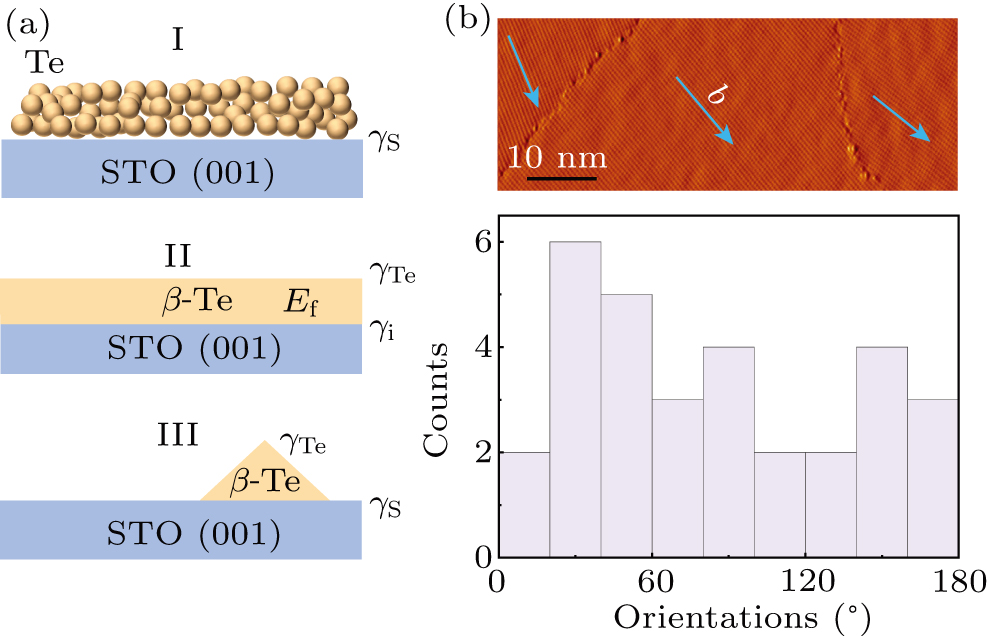
Above 7 ML, although the lower part (≤ 7 ML) of the film is flat and continuous, the additional Te atoms on the flat 7-ML film crystallize in a 3D manner (not shown), probably because of the enhanced diffusion of Te atoms on top of thick Te films. A more delicate annealing process is needed to keep the temperature below the diffusion temperature of Te atoms on thicker films and above the crystallization temperature. In addition, the orientations of domains in the Te-film seem random, without any preferred directions that register the in-plane lattice direction of the substrate. Figure 4(b) (upper one) shows the typical domain structures of the a-few-monolayer β-Te films on the STO (001) substrate by the LT/FA approach. Figure 4(b) (lower one) displays the statistics of orientations of the domains in Fig. 3(b), indicating the nearly random orientations of the Te domains. It is understandable because the substrate and the film have different lattice symmetries (the substrate is square while the β-Te film is rectangular). Furthermore, although the theoretically-proposed square phase matches better with the STO (001) substrate (1% mismatch), the as-grown films are always in the β phase (rectangular) probably because the square phase may only exist in some very special conditions.
In summary, we investigate the epitaxial kinetics of Te films growth on the SrTiO3 (001) substrate. By adopting the LT/FA approach, we achieve the successful growth of Te films with a nearly complete coverage and a uniform thickness, which is impossible by normal growth methods. This is accomplished by depositing Te atoms at liquid nitrogen temperature to freeze the diffusion of Te and doing post-annealing to crystallizing the amorphous film. This kind of approach circumvents the thermodynamic limitations that always lead to the VW growth mode of Te on various substrates. The thermodynamics in the LT/FA process also leads to the critical-thickness behavior, that is, the flat films only form above 3 ML. In addition, we find unusual large forbidden gaps (∼ 1.4 eV) on the a-few-monolayer β-Te films, which are almost twice those grown on other substrates. The underlying mechanism for the large gap is open for further studies. Our work achieves ultra-thin Te films of high quality that may have potential applications in photoelectronics, and also presents a necessary approach to prepare ultra-thin flat films with similar kinetics and thermodynamics.
Critical behavior in the epitaxial growth of two-dimensional tellurium films on SrTiO3 (001) substrates
- Received Date: 02/03/2023
- Accepted Date: 09/03/2023
- Available Online: 01/05/2023
-
Key words:
- molecular beam epitaxy /
- ultra-thin films /
- electronic structure
Abstract: Materials’ properties may differ in the thin-film form, especially for epitaxial ultra-thin films, where the substrates play an important role in their deviation from the bulk quality. Here by molecular beam epitaxy (MBE) and scanning tunneling microscopy/spectroscopy, we investigate the growth kinetics of ultra-thin tellurium (Te) films on SrTiO3 (STO) (001). The MBE growth of Te films usually exhibits Volmer–Weber (VW) island growth mode and no a-few-monolayer film with full coverage has been reported. The absence of wetting-layer formation in the VW growth mode of Te on STO (001) is resulted from its low diffusion barriers as well as its relatively higher surface energy compared with those of the substrate and the interface. Here we circumvent these limiting factors and achieve the growth of ultra-thin β-Te films with near-complete coverages by driving the growth kinetics to the extreme condition. There is a critical thickness (3 monolayer) above which the two-dimensional Te films can form on the STO (001) substrate. In addition, the scanning tunneling spectra on the ultra-thin Te film grown on STO exhibits an enormously large forbidden gap compared with that grown on the graphene substrate. Our work establishes the necessary conditions for the growth of ultra-thin materials with similar kinetics and thermodynamics.
 DownLoad: