
 首页
首页 登录
登录 注册
注册


HTML
-
The implementation of silicon carbide (SiC) based power devices is crucial for fulfilling the growing power consumption needs.[1–3] In order to fabricate these devices, a gate oxide with high quality and integrity is essential. This gate oxide functions as an insulating layer, allowing the gate to endure high transverse electric fields for the purpose of modulating channel conductance. Poor oxide quality and integrity can result in current leakage, which has a detrimental impact on device performance.[4–6] Currently, thermal nitride SiO2, which boasts ultra-low leakage current, is widely utilized as the material for the gate oxide.[7–9] Nevertheless, its relatively low dielectric constant compared to the SiC substrate can result in electrical breakdown prior to the SiC breakdown field being reached, hindering its suitability for high-power applications. Additionally, it is found that traditional thermal-oxidation methods for SiO2 often result in poor quality interfacial contact, leading to an abundance of interface defects and hindering device mobility.[10,11]
In the context of improving the electrical performance of power devices based on 4H-SiC, the use of a high-k oxide as a replacement for the traditionally employed thermal nitride SiO2 gate oxide has been proposed.[12,13] Under identical conditions of gate oxide thickness and gate voltage, a high-k dielectric material exhibits higher electron density and greater current-carrying capacity in inversion mode. Among the candidates for high-k oxides, Al2O3 has been identified as a promising material due to its high dielectric constant.[14,15] However, the use of high-k oxides comes with a challenge. A reduction in the energy band gap of the oxide may result in a reduction of the conduction and valence band offsets between the oxide and SiC, leading to an increase in the leakage current through the oxide.[16,17] This increase in leakage current could result in the breakdown of the dielectric layer. To mitigate this issue, a thin buffer layer of nitride SiO2, with a higher band offset, has been interposed between the high-k oxide and SiC substrate. Despite the numerous studies reporting on the electronic and structural properties of pure Al2O3 and stacked Al2O3 gates based on 4H-SiC, there is a lack of detailed analysis of the current conduction mechanisms and saturation thickness in these structures.[15,18–20]
In this investigation, the suitable thickness of the inserted SiO2 layer was established by evaluating the breakdown voltage and interface defects of an Al2O3 gate stack created through atomic layer deposition on 4H-SiC n-type material. This was accomplished by measuring the current–voltage and high-frequency capacitance–voltage of metal–oxide–semiconductor test structures comprised of 35 nm thick Al2O3 stacked on top of nitride SiO2 of varying thicknesses ranging from 0 nm–9 nm. The results suggested that the electric field and the thickness of the nitride oxide have a significant effect on the current that passes through the oxides. Ultimately, a maximum stacked SiO2 thickness was proposed that is ideal for ensuring breakdown and offset of the interfacial band.
-
MOS capacitors were fabricated on n-type, Si-faced, 4H-SiC substrates with a 10 nm thick epilayer doping level of 8 × 1015 cm−3 as test structures. As shown in Fig. 1(a), the purchased SiC was cleaned by a standard RCA process before thermal oxidation. The RCA method was carried out by dividing the SC1 and SC2 processes.[21] The RCA method removed organic contaminants by immersing the silicon wafer in NH4OH/H2O2/H2O (1:1:5 vol%) solution at 80 °C for 10 min. After removal, inorganic contaminants were removed by immersing the wafer in a solution of HCl/H2O2/H2O (1:1:5 vol%) at 70 °C–80 °C for 10 min. To remove the native oxide formed on the wafer during RCA cleaning, the silicon wafer was immersed in 0.5 vol% hydrofluoric acid (HF) solution for 1 min. The cleaned SiC wafer was rinsed with DI water. The nitride oxide was grown in an O2 ambient at 1350 °C in a thermal oxygen furnace. The nitride oxide thicknesses were obtained by adjusting the oxidation time. After oxidation, the furnace was cooled down to 1250 °C and nitride in a 10% NO ambient before the samples were removed. These samples, together with a clean wafer without nitride oxide, were inserted into a traveling-wave-type atomic-layer-deposition setup. By controlling the cycles of precursor Al(CH3)3 and oxidant O2, a 35 nm thick Al2O3 was deposited on the samples. The detailed atomic-layer-deposition process had been described elsewhere. After the deposition of the high-k oxide, a layer of poly-Si gate electrode was deposited on the top of the Al2O3 using low pressure chemical vapor deposition (LPCVD). An array of 1.13 × 10⁻⁴ cm2 area capacitors were then patterned using a photolithography process. Finally, after removing the back oxide, a large area of nickel, acting as a back contact, was sputtered on the n+ substrate.
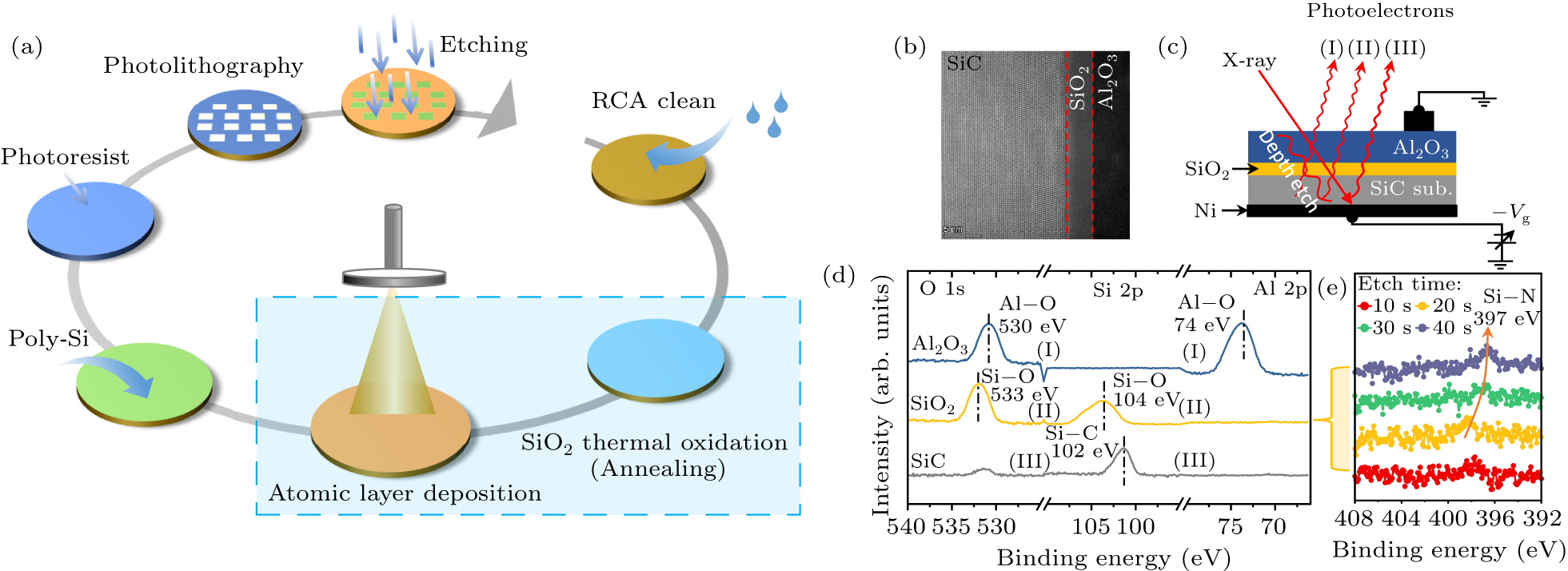
As seen in Fig. 1(b), a transmission electron microscopy (TEM) image of the prepared MOS stack showed that the Al2O3 and SiO2 were amorphous and the reaction at their interface was negligible. Note that the TEM contrasts of Al2O3 and SiO2 were at the same level. To understand the specific element distribution of the MOS capacity, the x-ray photoelectron spectroscopy (XPS) measurements were carried on the 35 nm thick Al2O3 stacked on nitride SiO2, as illustrated in Fig. 1(c). Figure 1(d) displays the photoelectron spectra of Al 2p, Si 2p, and O 1s, revealing the major components of the sample to be Al2O3, SiO2, and SiC. Notably, distinct bands corresponding to Al–O, Si–O, and Si–C are clearly visible. Additionally, we investigated the presence of nitride in the SiO2 films by varying the etching time from 10 s to 40 s and analyzing the N 1s position. A minor peak at 397 eV was observed near the SiO2–SiC interface, which can be attributed to the Si–N peak, providing evidence for nitride formation.[22] Based on these observations, we concluded that the 35 nm thick Al2O3 layer deposited on the nitride SiO2 substrate is well-constructed.
To understand the role of intercalated SiO2, we first select pure SiO2 and Al2O3 dielectric layer devices to test the interfacial state defects and dielectric breakdown characteristics. Figure 2(a) shows CV spectra of Al2O3 MOS capacitors measured at room temperature and at 1 kHz and 1 MHz frequencies. The gate bias is swept from depletion (negative bias) to accumulation (positive bias) and the capacitance signal for both frequencies is recorded simultaneously at each gate bias point. The dielectric constant of Al2O3 sample deduced from the capacitance in accumulation (5 V) is about 8. A first estimate of the interface trap density is extracted from the frequency dispersion of C–V curves. In the case of the reference SiO2 sample, dispersion is hardly visible indicating a rather low interface state density. As a comparison, the dispersion in ALD growth Al2O3 sample is much larger, revealing a high density of interface states. In a word, the pure ALD growth Al2O3 sample shows a limited band offset between the oxide and SiC, leading to a high density of interfacial states and an increase in the leakage current through the oxide.
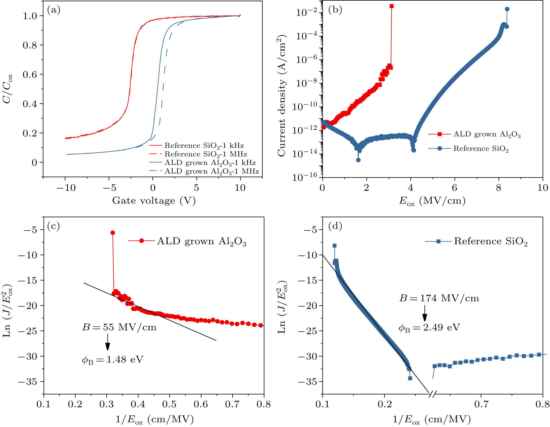
The MOS capacitors are investigated by I–V as well at room temperature. Leakage current density vs. electric field (J–E) curves for pure SiO2 and Al2O3 dielectric MOS capacitors are shown in Fig. 2(b). The thermal oxidated SiO2 has a breakdown field (∼9 MV/cm) which is higher than the ALD grown Al2O3 films (<4 MV/cm). This value of the breakdown field is below half the breakdown field achieved in the reference SiO2/SiC MOS capacitor. Besides, in that study, the leakage current density prior to breakdown is of the order of 10−7 A/cm2 which is a few orders of magnitudes higher than in the reference SiO2/SiC MOS capacitor, which could be the trigger for the degradation of the Al2O3 dielectric layer. Significant Fowler–Nordheim (F–N) tunneling is seen in the J–E profile of the sole ALD Al2O3 and reference SiO2 MOS sample. Therefore, the J–E response of these MOS samples is analyzed further using the F–N tunneling mechanism to determine the tunneling barrier height. F–N tunneling current density[23] across MOS devices at high field is described by
where
The parameters A and B depend on the tunneling barrier height ϕB and the effective mass of the tunneling electron mox in the oxide. A and B, can be derived from the experimental I–V characteristics plotted as ln(J/E2) vs. 1/E, a so-called F–N plot. The slope of the straight line at high electric fields gives B while A is determined from the intercept. Since B is the exponent in the equation for F–N tunneling current density, it is the prominent parameter in determining the current flow in the gate oxide. Figures 2(c) and 2(d) show an F–N plot for an ALD grown Al2O3 and for a reference thermal oxidating SiO2. The value of parameter B is 55 MV/cm and 174 MV/cm for Al2O3 grown by ALD and for reference SiO2, respectively. The effective barrier height for the ALD grown Al2O3/4H-SiC interface extracted from this analysis is 1.48 eV by taking the effective electron mass in Al2O3 to be 0.2mo, where mo is the free electron mass.[24] A SiO2/4H-SiC barrier height of 2.49 eV is obtained by assuming mox in SiO2 is 0.42mo. This barrier height of the reference SiO2/4H-SiC MOS sample is reasonably close to the previously reported values for dry SiO2 determined by the F–N tunneling mechanism. As for amorphous ALD grown Al2O3/4H-SiC, the highest barrier height in literature determined by the F–N tunneling mechanism is 1.18 eV which is far from 1.58 eV for ideal Al2O3 films. In our work, the extracted barrier height is 1.48 eV close to that of ideal Al2O3 films. This result indicates that the Al2O3 is well growth.
As a comparison, the capacitance–voltage (C–V) characteristics of 35 nm thick Al2O3 stacked on 0 nm, 3 nm, 6 nm, or 9 nm thick nitride SiO2 were investigated. The films were analyzed for their interfacial state defects and dielectric breakdown characteristics. Capacitance–voltage spectra were obtained at room temperature and at both 1 kHz and 1 MHz frequencies. The gate bias was swept from depletion (negative bias) to accumulation (positive bias), and the capacitance signal for both frequencies was recorded simultaneously at each gate bias point. The results from the C–V analysis were used to study the effect of nitride SiO2 intercalation on Al2O3 samples. The C–V results in Figs. 3(a)–3(c) showed a significant reduction in the difference between high and low frequencies of the intercalated samples compared to pure Al2O3 samples. This improvement was attributed to the effective improvement of interfacial contact and reduction in interfacial state defects due to the introduction of nitride SiO2. The C–V results were further analyzed to extract the interfacial state defects at different energy states as shown in Fig. 3(d), and the results showed a significant decrease in the interfacial state defects in the intercalated samples. Additionally, the concentration of interfacial defects was found to increase with the increasing thickness of the SiO2 samples, and it was hypothesized that a longer annealing time may be necessary to fully passivate the SiO2–SiC interface as the thickness of SiO2 increases. However, as the SiO2 layer thickness increases, the annealing process became more challenging, requiring longer time and higher temperatures, leading to higher production costs.
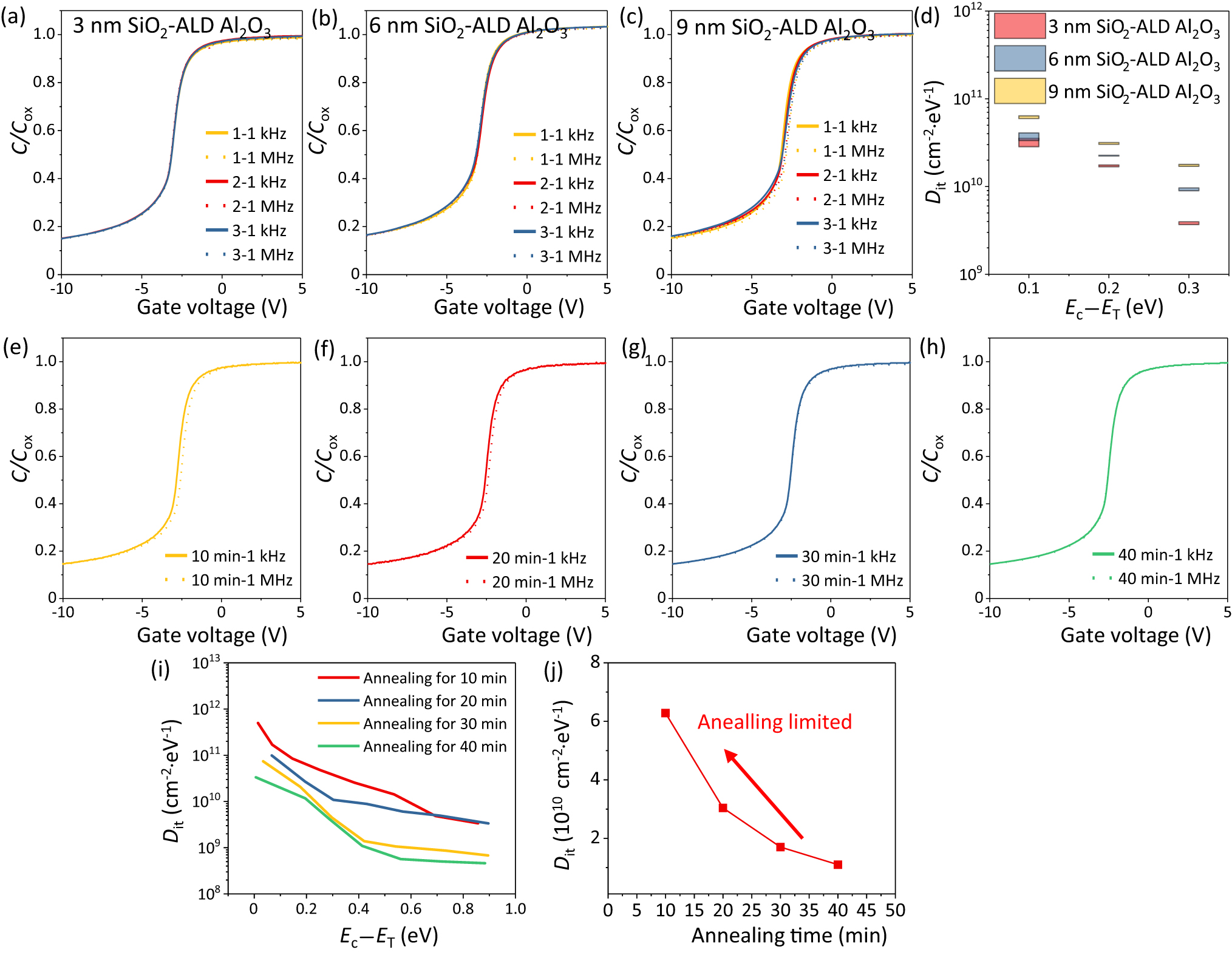
To better explain this phenomenon, we continue to do additional experiments to figure out the relationship between the annealing time and the density of interface state. As shown in Figs. 3(e)–3(h), we test the capacities of samples with increasing annealing time. Based on our experimental results as shown in Fig. 3(i), we have found that increasing the annealing time from 10 min to 40 min leads to a significant reduction in the density of interface states (Dit) at the SiO2–SiC interface. Specifically, we observed a decrease in Dit from approximately 6 × 1010 cm−2⋅eV−1 to 2 × 1010 cm−2⋅eV−1. These results reveal a clear relationship between annealing time and Dit, demonstrating that longer annealing times are necessary to fully passivate the SiO2–SiC interface as the thickness of the SiO2 layer increases, as shown in Fig. 3(j). Our findings provide strong evidence for the effectiveness of extended annealing times in reducing the density of interface states at the SiO2–SiC interface. We suggest that this effect arises from the thermal activation of oxygen species within the oxide layer, which helps to heal defects and improve the structural quality of the interface.
Moreover, a SiO2 layer was introduced on top of SiC to increase the band offset between Al2O3 and SiC. The electrical performance of the metal–oxide–semiconductor (MOS) capacitors was evaluated through current–voltage measurements performed at room temperature. The results, displayed in Fig. 4(a), showed that the effective breakdown field, determined using the equation Eeff = VG–VFB/tox,total, where VG is the gate voltage, VFB is the flatband voltage, and tox,total is the total thickness of the dielectric stack, was in the range of 6 MV/cm–9 MV/cm. The leakage current was observed to be relatively low at around 10−11 A/cm until a sharp increase was observed when the electric field reached 5 MV/cm. Additionally, the breakdown field across the Al2O3 dielectric could be estimated by considering the difference of dielectric constants in the stack using a mathematical expression
The expression used in this study calculates the capacitances of SiO2 and Al2O3 (Cox,SiO2 and Cox,Al2O3) based on their respective dielectric constants and thicknesses. The resulting breakdown field was determined to be approximately 6.5 MV/cm, with no significant effect on the breakdown field of the Al2O3 dielectric caused by the insertion of the SiO2 intercalation layer. This highlights the advantage of using the stack dielectric MOS capacitor in applications where higher gate voltage operation is required.
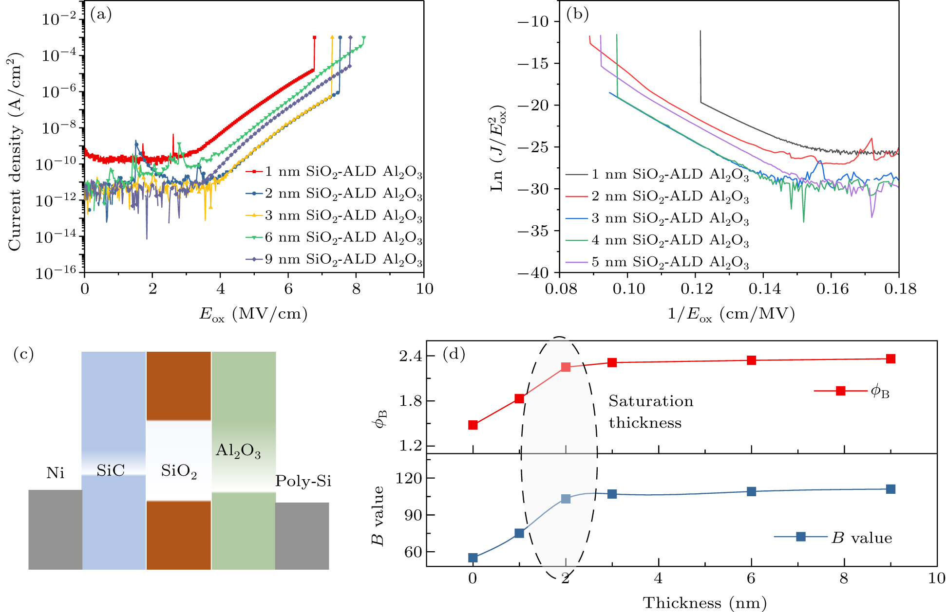
The impact of the inserted SiO2 on the interface barrier was also evaluated through the Fowler–Nordheim tunneling measurements. The F–N plots for Al2O3 stacked with different thicknesses of SiO2 samples were compared with both the ALD grown Al2O3 and the reference thermal oxidized SiO2, as shown in Fig. 4(b). The value of the parameter B was determined to be 75 MV/cm for a 35 nm thick Al2O3 stack on a 1 nm thick nitride SiO2, 103 MV/cm for 2 nm, 107 MV/cm for 3 nm, 109 MV/cm for 6 nm, and 111 MV/cm for 9 nm thick nitride SiO2. The effective barrier height, as determined by F–N tunneling, was extracted to be 1.83 eV for the 35 nm Al2O3 stack on 1 nm SiO2, 2.25 eV for 2 nm, 2.31 eV for 3 nm, 2.34 eV for 6 nm, and 2.36 eV for 9 nm thick nitride SiO2. For SiO2 thicknesses above 2 nm, the barrier heights of the Al2O3/SiO2/4H-SiC MOS samples were observed to be similar to those of dry SiO2 (< 10%), as determined through F–N tunneling, as shown in Fig. 4(c). The findings of the study suggested that beyond a thickness of approximately 2 nm, there is a saturation in the widening of the energy band offset between Al2O3 and SiC caused by the insertion of the SiO2 intercalation layer.
In this study, the thickness impact of inserted SiO2 on the interfacial properties of metal–oxide–semiconductor samples was investigated and found to have a significant influence. Firstly, with regard to the minimization of interfacial defect concentration, it was observed that the insertion of a SiO2 layer effectively improved the interfacial properties as compared to single-layer Al2O3 samples. However, as the SiO2 layer thickness increases, the annealing process became more challenging, requiring longer time and higher temperatures, leading to higher production costs. Thus, it was concluded that the SiO2 layer thickness should be kept as thin as possible for optimal results. In addition, the effect of SiO2 thickness on the gate current breakdown characteristics of MOS samples was also explored. The results showed that an increased SiO2 layer thickness led to a lower gate current and a higher breakdown voltage, due to the widening of the energy band offset between Al2O3 and SiC. This improvement in the gate dielectric layer’s reliability was a result of the SiO2 intercalation layer. Remarkably, it was noted that there exists a saturation point in the SiO2 thickness requirement for voltage withstand reliability, observed to be around 1 nm–2 nm as shown in Fig. 4(d), which balances the control of interfacial defects and the improvement of gate current reliability. In conclusion, this study highlighted the crucial role of SiO2 insertion thickness on the interfacial properties of MOS samples and provided important insights for optimizing the design of such systems.
-
The optimal thickness of intercalated SiO2 in metal–oxide–semiconductor samples was determined by examining the influence of SiO2 thickness on the breakdown voltage and interfacial defects. This was accomplished through the investigation of atomic-layer-deposited Al2O3 gate stacks on different thicknesses of thermally nitride SiO2 on n-type 4H-SiC. The characterization of the MOS test structures was performed through current–voltage and high-frequency capacitance–voltage measurements. The results showed that the thickness of the nitride oxide and the applied electric field both impacted the current conducted through the oxides. Furthermore, a saturation thickness of approximately 1 nm–2 nm for the stacked SiO2 was proposed, as it contributed significantly to the dielectric breakdown and interfacial band offsets. This study sheds light on the critical importance of the thickness of intercalated SiO2 in MOS samples and provides valuable insights for optimizing the design of these systems. The findings of this study could be used as a guide for future research and development in the field of MOS devices. Under identical conditions of gate oxide thickness and gate voltage, a high-k dielectric material exhibits higher electron density and greater current-carrying capacity in inversion mode. The methods and techniques used in this study could also serve as a benchmark for similar studies investigating the impact of intercalated SiO2 thickness on the performance of MOS samples.
 DownLoad: