
 首页
首页 登录
登录 注册
注册


HTML
-
III-nitrides are promising semiconductor systems with widespread applications for power,[1,2] radio frequency (RF),[3,4] optoelectronic,[5,6] and light-emitting devices.[7,8] In general, most of the conventional III-nitride-based devices are epitaxially grown along the c-plane direction. However, a strong built-in electric field parallel to the c-direction induced by the spontaneous and piezoelectric polarization forces the spatial separation of electrons and holes in the quantum wells, causing a reduction of the recombination rate and a redshift of the emission wavelength in III-nitrides based light-emitting devices.[9,10] This general phenomenon, known as the quantum-confined Stark effect (QCSE), severely hinders the improvement of the internal quantum efficiency in nitride-based optoelectronic devices.[11] Currently, various methods for conquering the adverse effects of QCSE have been reported, such as the introduction of V-pits,[12] the employment of AlN/AlGaN strain-compensating layers,[13] the usage of stress engineering,[14] and the growth of InGaN quantum dots.[15] In fact, the adverse effects of built-in electric field could also be eliminated by growing nonpolar GaN-based materials, which means that the growth direction of semiconductor is perpendicular to the direction of electric field.[16,17] Apparently, the adverse effects of built-in electric field could be suppressed with various degrees when the angle between growth direction of semiconductor and the direction of electric field is varied from 0° to 90°, which are semipolar materials.[18] Thus, the study of nonpolar/semipolar GaN-based materials has increasingly received more attention.
Recently, the successful fabrications of semipolar (1–101)-plane,[19] (11–22)-plane,[20] and (20–21)-plane[21] GaN-based LEDs have been reported. Moreover, high bandwidth visible light communication has been reported by using semipolar (20–21)-plane[22] and (11–22)-plane[23] GaN-based LEDs. However, given the presence of apparent anisotropy in the growth surface of nonpolar materials, the epitaxial growth of nonpolar GaN-based materials is relatively difficult when compared to the polar/semipolar counterparts.[24] Although studies of nonpolar (10–10)-plane AlGaN,[25] GaN,[26] and InGaN,[27] and nonpolar (11–20)-plane AlGaN,[11] GaN,[28] and InGaN[29] have recently been reported, the research of nonpolar III-nitrides based devices is significantly behind. A reliable p-type semiconductor is necessary for a device with p–n junction. Although the successful growth of nonpolar p-GaN has been reported,[30] there is no detailed and in-depth study of the activation efficiency and activation energy of Mg acceptors in nonpolar p-type GaN.
In this paper, nonpolar a-plane p-type GaN epilayers with growth temperatures from 980 °C to 1010 °C were grown on r-plane sapphire substrate by a close coupled shower head (CCS) metal–organic chemical vapor deposition (MOCVD) system. The influence of growth temperature on structural anisotropy and electrical properties of nonpolar p-type GaN films were investigated intensively. Eventually, a p-type GaN with high activation efficiency and high doping concentration was obtained.
-
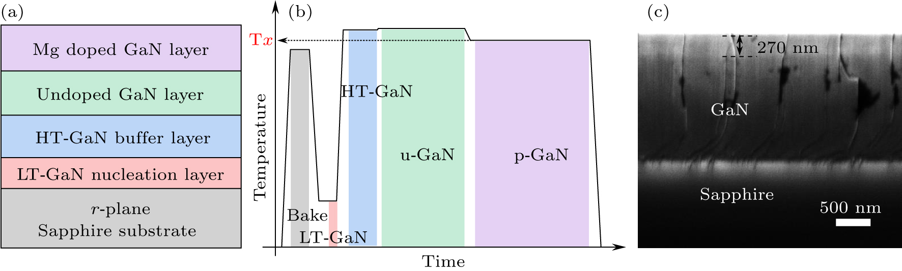
All the nonpolar (11–20) a-plane GaN samples were grown on semipolar (1–102) r-plane sapphire substrates by a CCS MOCVD system. Ammonia (NH3), trimethyl-gallium (TMGa), and bicyclopentadienyl-magnesium (Cp2Mg) were used as the N, Ga, and Mg source precursors, respectively, which were mainly introduced into the reaction chamber by hydrogen (H2) as a carrier gas. The pressure of the chamber was maintained at 53 mbar during the whole process. The schematic structure of the nonpolar p-type GaN samples prepared in this paper is shown in Fig. 1(a). Figure 1(b) shows the temperature changed with time in the corresponding process. Before growth, high-temperature baking and a nitridation process were carried out at 990 °C to remove the surface contamination of the sapphire substrate. Subsequently, a 20 nm-thick low-temperature GaN (LT-GaN) nucleation layer was deposited on the sapphire substrate at 550 °C and followed by a high-temperature GaN (HT-GaN) buffer layer grown at 1030 °C. Afterward, the temperature was raised to 1035 °C to grow an undoped GaN (u-GaN) layer on the HT-GaN layer. Finally, the Mg-doped GaN layers with various temperatures with a V/III molar flow ratio of 5000 were grown on the u-GaN layer to explore the influence of temperature on the morphology and electrical properties of nonpolar a-plane p-type GaN. Four nonpolar a-plane p-type GaN samples were grown in this work with 980 °C, 990 °C, 1000 °C, and 1010 °C, and were named samples T1, T2, T3, and T4, respectively. To activate the Mg dopants, all of the samples were rapidly thermally annealed at 800 °C for 10 min within a nitrogen ambient.
The surface morphologies of the p-type GaN samples were characterized by scanning electron microscopy (SEM) and atomic force microscopy (AFM). The crystalline quality analysis of the samples was mainly achieved by high resolution x-ray diffraction (HR-XRD). The in-plane strains of a-plane p-GaN samples were evaluated with the Raman spectra excited by a 514 nm laser at room temperature. The Hall effect measurements were employed to estimate the electrical properties of all of the samples. Specifically, the Ni (20 nm)/Au (20 nm) electrodes were deposited at the four corners of the surface of the square a-plane GaN sample by electron beam evaporation, and ohmic contact was formed between the metal and the sample after annealing at 500 °C for 10 min in an air environment. The Mg incorporation density was determined using secondary ion mass spectroscopy (SIMS) measurements.
-
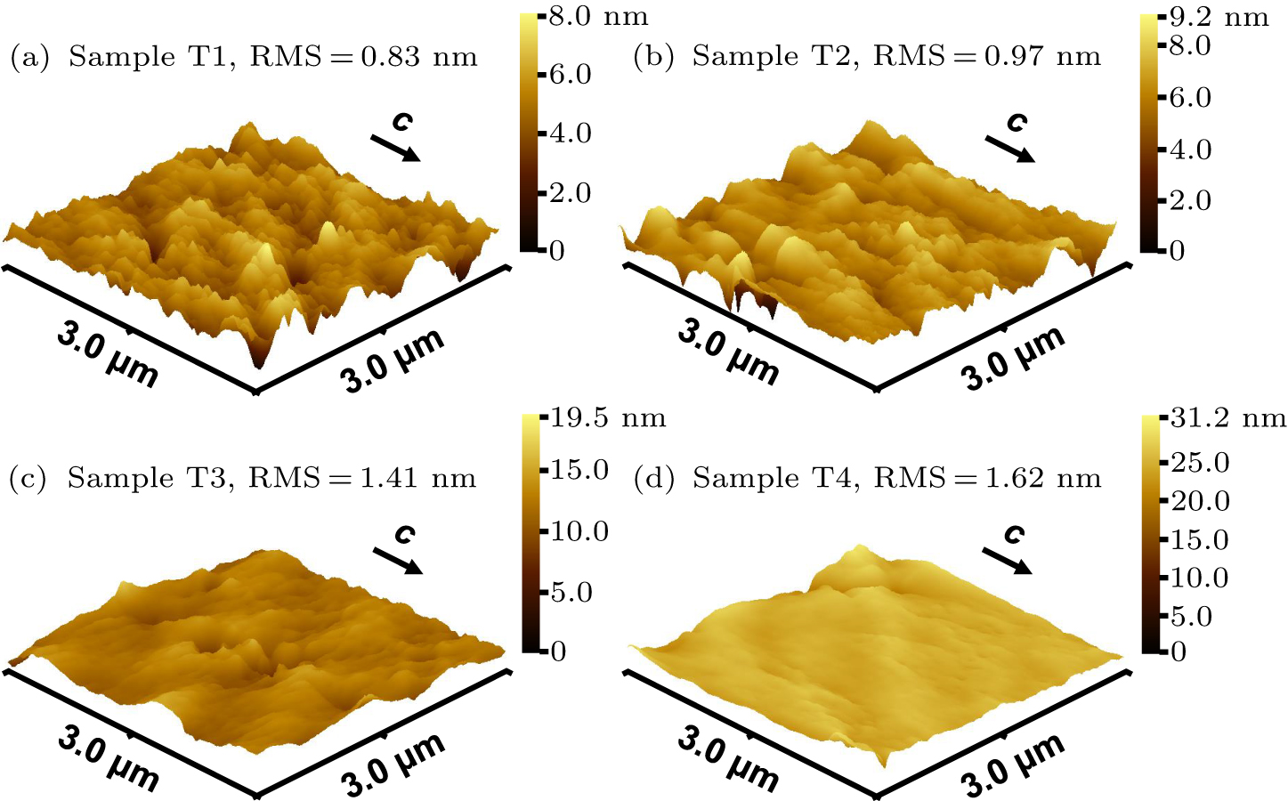
The cross-sectional SEM graph for the nonpolar a-plane p-GaN sample is shown in Fig. 1(c). The difference in conductivity between the Mg-doped layer at the top and undoped layer at the bottom results in a clear boundary at the interface. The thickness of the Mg-doped layer was determined to be 270 nm by both the cross-sectional SEM graph and the in situ reflectance monitoring system (not shown). The three-dimensional view AFM images of all a-plane p-GaN samples were measured in a detection area of 3 μm × 3 μm. It is evidently observed from Fig. 2 that the surface morphology of the four samples possesses an undulating structure that is distributed along the c-direction. This typical directional structure of nonpolar GaN is mainly related to the larger diffusion length of the Ga adatom along the c-direction than along the m-direction on the surface.[31] Samples T1 and T2 with 0.83 nm and 0.97 nm root mean square (RMS) roughness feature a smoother and flatter surface that is comparable to the previously reported Mg-doped nonpolar a-plane GaN.[32] In addition, for samples T3 and T4, the width of the undulating structure gradually increases and the corresponding RMS roughnesses are 1.41 nm and 1.62 nm, respectively. This phenomenon implies that a higher temperature might inhibit the in-plane surface diffusion of GaN along the m-direction[33] and promote the growth along the c-direction, resulting in the deteriorated surface morphology.
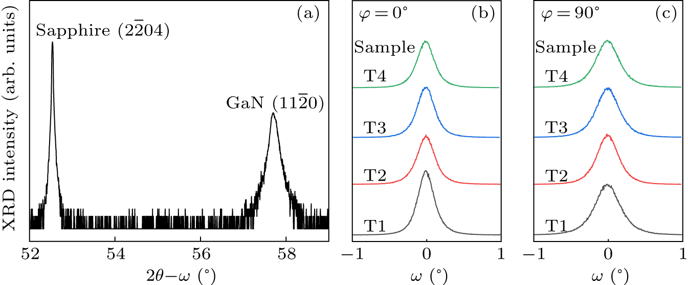
The XRD ω–2θ scanning curve of the sample is shown in Fig. 3(a). The diffraction peaks at 52.54° and 57.71° correspond to (2–204) r-plane sapphire substrate and (11–20) a-plane GaN, respectively.[11] This further indicates that nonpolar a-plane GaN has been successfully grown on semipolar r-plane sapphire substrate. The x-ray rocking curves (XRCs) based on 57.71° position were measured, respectively, at azimuth angles of φ = 0° (along c-direction) and φ = 90° (along m-direction) to describe the structural anisotropy of the nonpolar a-plane GaN samples. The full width at half maximum (FWHM) values for XRCs of the four samples can be obtained by a Gauss function fitting the XRCs, as shown in Figs. 3(b) and 3(c), and the results are summarized in Table 1. Significantly, the FWHM values of XRCs along c-direction are much smaller than those along the m-direction, which is due to the smaller lattice mismatch between the nonpolar a-plane GaN and the semipolar r-plane sapphire substrate along the c-direction.[34] Additionally, the FWHM values of XRCs along c-direction increased from 1019 arcsec for sample T1 to 1101 arcsec for sample T2, but decreased from 1515 arcsec to 1300 arcsec along the m-direction. This indicates that temperature has a great difference on the crystalline quality in both directions. To accurately evaluate anisotropy in crystalline quality, the anisotropy ratio A is defined by the following equation:
where F90 and F0 are the FWHM values of XRC measured at azimuth angles of φ = 0° and φ = 90°, respectively. The calculation results of samples T1–T4 are presented in Table 1. The anisotropy ratios reduced sharply from 19.6% for sample T1 to 8.3% for sample T2. This remarkable improvement of anisotropy in crystalline quality can be attributed to the release of residual stress between u-GaN layer and p-type GaN layer as the temperature increased.[35] On the contrary, the anisotropy ratio increased significantly from 8.3% for sample T2 to 14.0% for sample T4. Although relatively high temperatures can promote the incorporation of Mg atoms,[35] an excess of Mg atoms can result in lattice distortion and an increased density of defects, particularly nitrogen vacancies, in the p-GaN layer.[34] The presence of excessive nitrogen vacancies can strengthen the self-compensation effect, leading to a decrease in the concentration of the holes. As a result, an 8.3% of low anisotropy in crystalline quality could be obtained at 990 °C by optimizing the growth temperature.
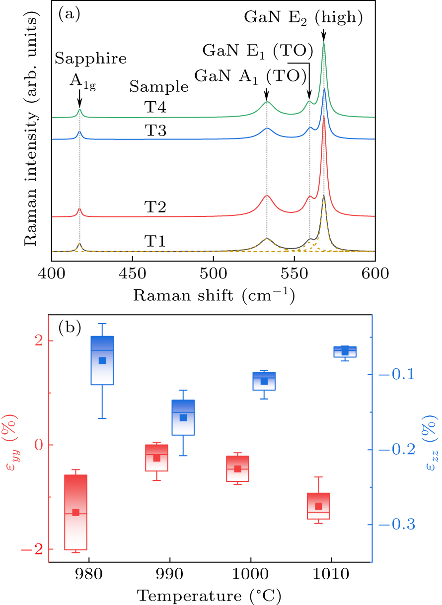
The Raman spectra of the p-type a-plane GaN films prepared at different growth temperatures were carried out to investigate the strain state. As shown in Fig. 4(a), the Raman peaks for all of the samples located at 418 cm−1 belong to A1g mode of r-sapphire and the peaks observed at 532 cm−1, 559 cm−1, and 568 cm−1 correspond to A1 (TO), E1 (TO), E2 (high) mode of GaN, respectively.[36] In general, the biaxial in-plane strain ε along x, y, and z axis for nonpolar a-plane GaN film can be expressed as[36]
where C11, C12, and C13 are all the elastic stiffness constants and the x, y, and z axis are defined as GaN [11–20], [1–100], and [0001]-directions, respectively. Furthermore, the relationship between Raman peak shifts Δω and in-plane strain can be described as[36]
Here λ represents a certain Raman mode and aλ, bλ, and cλ are all the phonon deformation constants for the above homologous mode. Independent peaks, which are shown as the yellow dotted line in the Fig. 4(a), can be obtained by Lorentz fitting Raman spectra so as to accurately extract the peaks positions. The relative displacement of peak position can be calculated according to the strain-free phonon frequencies of E1 (TO) (558.8 cm−1) and E2 (high) (567.6 cm−1) modes. The in-plane strains εyy and εzz are estimated by solving Eqs. (2) and (3). In order to correctly describe the in-plane strains of all of the samples, the Raman spectra at four positions were measured for each sample under the same conditions. Figure 4(b) gives a box-type statistical diagram of the calculated in-plane strains as a function of growth temperature. It is clearly noted that all of the samples suffered compressive strain along the c- and m-directions,[37] and the values of compressive stress in c-direction are less than those in the m-direction. Interestingly, the strain variations along c- and m-directions for samples T1–T4 are consistent with the trend of the FWHM values of the XRCs. This means that an increase or decrease in stress can be judged by an increase or decrease in the FWHM value of XRC, which indicates that the crystal quality seriously restricts the stress value.
The AC Hall effect measurement at room temperature was used to reliably determine the carrier type of Mg-doped nonpolar a-plane GaN films, as shown in Fig. 5(a). The hole concentrations after annealing were determined to be 4.1 × 1017 cm−3, 1.3 × 1018 cm−3, 5.9 × 1017 cm−3, and 5.5 × 1017 cm−3 for samples T1, T2, T3, and T4, respectively, suggesting that all of the films achieve Mg activation and p-type semiconductor. Meanwhile, hole concentrations as the temperature increased first increased and then decreased. The contrary variation of carrier mobility was ascribed to the enhanced ionized impurity scattering caused by a relatively high hole concentration. It can be found that a hole concentration of 1.3 × 1018 cm−3 for sample T2 was achieved with a relatively smooth surface morphology (as shown in Fig. 2(b)), a low anisotropy in crystalline quality (as shown in Table 1), and small strains (as shown in Fig. 4(b)). Naturally, the carrier mobility of sample T2 was decreased evidently due to its high hole concentration.
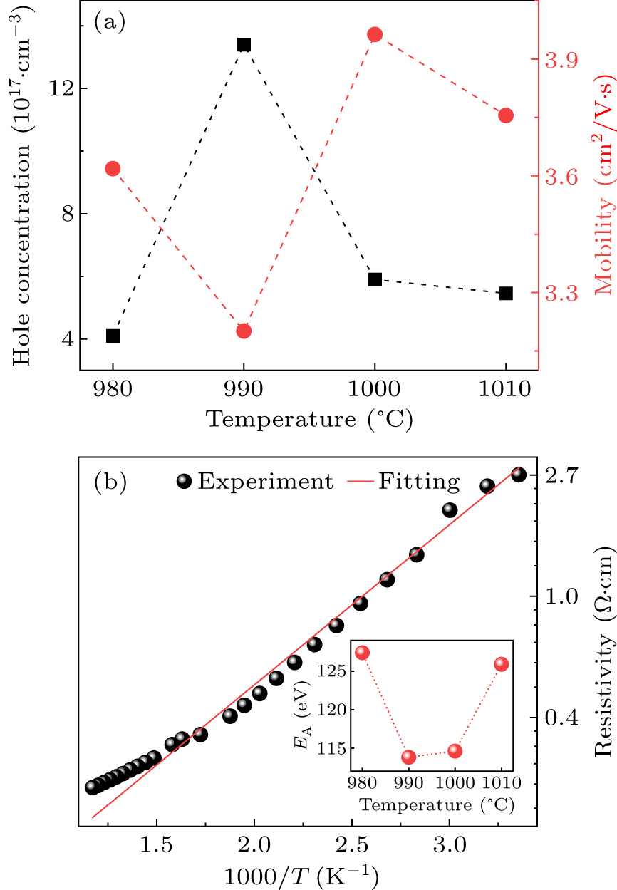
To explore the transmission characteristics of the carriers, we performed temperature dependent Hall-effect measurements on sample T2 from 298 to 853 K. From the resistivity as a function of reciprocal temperature in Fig. 5(b), it is obvious that the sample presents a typical thermally activated conduction process.[38] The resistivity decreases with increasing temperature, whereas hole concentration is positively correlated with temperature. The acceptor activation energy (EA) can be deduced by fitting the measurement data with Arrhenius-type formula.[39] The inset shows the relationship between activation energy and temperature. The calculated EA values of all nonpolar a-plane GaN samples are smaller than that reported in the c-plane GaN (174 meV).[40] It can be inferred from this that the heavy hole band in nonpolar GaN would upward shift due to its strain anisotropy, so the Mg acceptors energy level will become shallower accordingly. Thus, the activation energy of Mg acceptors in nonpolar GaN is obviously smaller than that in polar GaN.
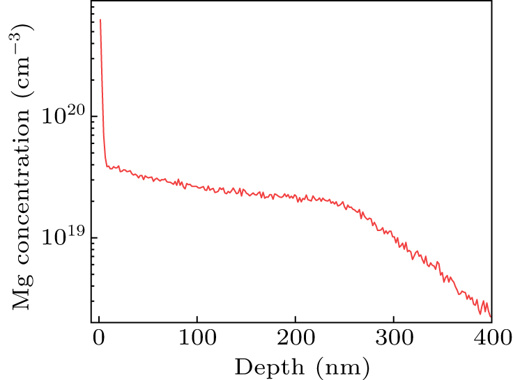
A SIMS measurement of sample T2 was recorded to confirm the Mg-doping concentration of Mg atoms into the GaN film, as shown in Fig. 6. The Mg concentration signal increased along the growth direction and the strongest signal appeared near the surface of the sample, which could be explained by the Mg memory effect.[41] The significant Mg concentrations (> 1.5 × 1019 cm−3) are observed at profile depth < 270 nm. This is in agreement with the SEM results. Furthermore, the Mg-doping efficiency is defined as the ratio of the hole concentration and Mg-doping density (Hall/SIMS ratio). Here, the average Mg concentration is 2 × 1019 cm−3 in the p-type GaN layer of sample T2 and the Hall/SIMS ratio is calculated to be as high as 6.5%, indicating that the optimized temperature can significantly suppress the self-compensation effect to effectively increase the hole concentration and activation rate.
-
We have grown nonpolar a-plane p-type GaN with different Mg-doping temperatures on two-inch semipolar r-plane sapphire substrates by the MOCVD system. The sample with 0.97 nm RMS roughness at an optimized temperature of 990 °C reveals high crystalline quality, relatively low in-plane strains, and high hole concentrations of 1.3 × 1018 cm−3. It is revealed that the variation trend of the XRC FWHM values along the c- and m-directions are essentially consistent with the stress along the corresponding directions. Temperature dependent Hall measurements show that the acceptor activation energy is 114 meV at a growth temperature of 990 °C. It is of note that a Mg activation efficiency as high as 6.5% has been achieved in this work by optimizing the growth temperature of the Mg-doped layer.
 DownLoad: