
 首页
首页 登录
登录 注册
注册


HTML
-
Two-dimensional (2D) layered materials have attracted considerable interest in recent years owing to their potential applications in nanomaterials and optoelectronics.[1–6] In addition to a variety of materials and the dependence of layer thickness, stacking 2D layers into artificial van der Waals heterostructures also provides degrees of freedom to engineer their electronic and optical properties.[7,8] The resulting modulated strain field and electrostatic potential combined with the ubiquitous interlayer coupling may give rise to distinct emergent physical properties,[23–26] for example, the Hofstadter butterfly spectra,[17,27–29] cloned Dirac Fermions,[17–19] fractional quantum Hall effects[28–30] and topological mosaics[31] in graphene-based and transition metal dichalcogenides-based Moiré superlattices (MSLs). Thus far, researchers have realized the MSLs fabrication by wet transfer of mechanically exfoliated monolayers,[32–35] epitaxial growth,[36–38] one-pot solvothermal approaches,[39] and so forth. The commonly used method to fabricate MSLs through stacking together mechanically exfoliated monolayers suffers from issues of uncontrolled stacking patterns and registry, contamination at the interfaces, and sample uniformity/size limitations.[32–35] Recently, epitaxial growth approach (e.g., chemical vapor deposition) can in principle overcome these problems, but are not yet widely reported.[36–38] Here, we suggest that the spiral dislocation driven growth is another desirable method for the preparation of high quality MSLs samples.
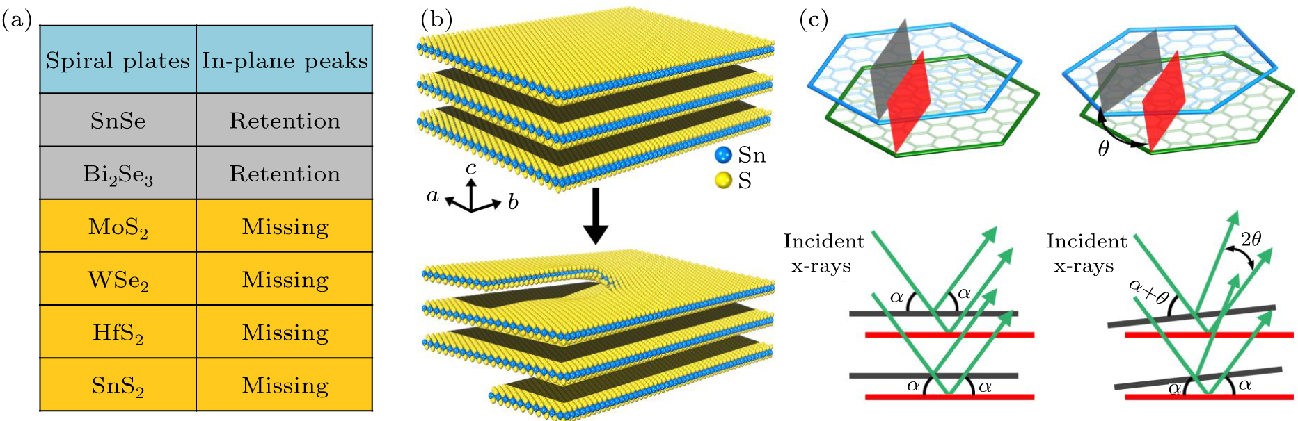
In addition to layer-by-layer growth, a series of 2D spiral structures have been recently driven by screw dislocations under low supersaturation condition (Fig. 1(a)).[39–49] Careful structural and spectroscopic analysis revealed that these spiral structures possess a variety of stacking patterns, such as triangular, tetragonal, hexagonal, and triangular–hexagonal mixed shapes. A schematic representation of the incorporation of screw dislocation from layer-by-layer structure to spiral structure is shown in Fig. 1(b). Through the investigation of these cases, except for SnSe and Bi2Se3, almost all in-plane x-ray diffraction (XRD) peaks of these compounds are missing. Based on high-resolution transmission electron microscope and second-harmonic generation measurements, Fan et al. identified that a twist angle of 5° is formed between the top and bottom layers in spiral WS2.[42] Additionally, the selected area diffraction measurement clearly shows two sets of diffraction spots with angles ranging from 1.6° to 3° occurred in spiral BiOCl.[39] Thus we speculate that the peaks missing in XRD spectra should be attributed to the appearance of small twist angle in the spiral plates. As illustrated in the left panel of Fig. 1(c), the same diffraction angle in the layer-by-layer growth structure will cause the superimposition of diffraction intensity for a given lattice plane. On the contrary, the appearance of twist angle (θ) between two adjacent spiral layers breaks the in-plane lattice periodicity, losing the ability to superimpose the in-plane diffraction intensity (right panel of Fig. 1(c)). However, its periodicity along out-of-plane direction is maintained with the growth of spiral plates, causing the relative diffraction intensity of in-plane peaks to visually decrease to a negligible level. Hence we believe that MSLs can be obtained through screw dislocation driven growth with a processing method to form a small twist angle. An easy way to confirm its formation is by checking the disappearance of in-plane peaks in the XRD spectra of synthesized spiral plates. To be more precise, one can intuitively observe the explicit atomic arrangements of selected regions by performing scanning transmission electron microscope analysis.[38,39]
In this work, we take SnS2 MSL as an example to investigate its electronic and optical properties. Xia et al. successfully synthesized a large scale of 2D spiral SnS2 crystals by using a simple atmospheric pressure vapor deposition method.[46] The good photo-stability and reproducibility as well as a fast photoresponse time enable the SnS2 to be a promising candidate for photodetectors. The in-plane peaks missing in its XRD spectrum indicate the existence of a small twist angle. On the other hand, the diffraction reflections indexed to (000N) (N = 0, 1, 2, …) planes have the same diffraction angles as bulk SnS2, which denotes that the spiral SnS2 crystals grow preferably along out-of-plane direction with the same interlayer distance as bulk SnS2. Hence we conclude that the SnS2 MSL with a constant interlayer distance has been synthesized. However, the large wavelength of the Moiré potential results in great MSL complexity, posing challenges for both theoretical and experimental investigations of its properties. Theoretically speaking, it is very challenging to use a large unit cell for electronic structure calculations with density functional theory (DFT). In addition to the most commonly used tight binding-based method,[50–54] large-scale DFT simulations based on linear combination of atomic orbitals or linearly scaling 3D fragment methods have also been used for the investigation of MSLs.[55–58] However, the MSL period reaches the order of tens of nanometers under a small lattice mismatch or small twist angle,[14,38,39,50,55,59–61] which is dozens of times that of common crystals. In addition to the fascinating properties of MSLs as a whole, the property variations at different local positions within the MSLs are also important for the understanding of material characteristics. In this work, we recommend another method to simulate the property variations throughout the MSL, which has consistently described the experimental observation of spiral BiOCl.[39] We note that our method is only suitable for the investigation of MSL with a small twist angle.
-
First-principles calculations were carried out within the framework of density functional theory by using plane-wave pseudopotential methods as implemented in the Vienna Ab-initio Simulation Package.[62,63] The electron–ion interactions were described by using the projected augmented wave pseudopotentials with the 5s25p2 (Sn) and 3s23p4 (S) treated explicitly as valence electrons. We used the generalized gradient approximation formulated by Perdew, Burke, and Ernzerhof[64] as the exchange–correlation functional. The layered SnS2 structures were embedded in a vacuum region with 30 Å thickness. A kinetic energy cutoff of 520 eV was used for wave-function expansion, and a 31 × 31 × 1 k-point grid within the Monkhorst–Pack scheme was adopted for electronic Brillouin zone integration. The optB86b-vdW functional[65] was used to describe the dispersive van der Waals interaction, which was found to give a good agreement with experimental lattice parameters.[66] The cell parameters and internal atomic positions were obtained using the conjugate gradient technique until the total energies converged to less than 10−5 eV. The interlayer distance of the constructed SnS2 structures was fixed at 0.592 Å (the same interlayer distance as bulk SnS2)[66] during the structure optimization.
-
To give an intuitive impression of SnS2 MSL, a topological SnS2 bilayer structure with 3.1° twist angle is constructed as shown in the perpendicular view in Fig. 2(a). When two adjacent spiral layers form a small twist angle θ, the period L of such MSL is given by L = a0/sin θ ≈ a0/θ, where a0 is the length of in-plane Bravais lattice (0.365 Å for SnS2).[66] This leads to the formation of a periodic MSL structure with a period 6.75 nm, containing 662 SnS2 units (1986 atoms). The periodic length will significantly increase if a smaller twist angle is formed in the spiral structure. For example, the periodicity is 20.91 nm when θ = 1.0°, which contains more than 1.9 × 10⁴ atoms in SnS2 MSL. To avoid the costly calculations, it is necessary to find an easier way to investigate the electronic properties of SnS2 MSL. Another problem is the non-negligibly internal properties of such a large structure, which deserves an in-depth study to deepen the understanding of MSL structures.
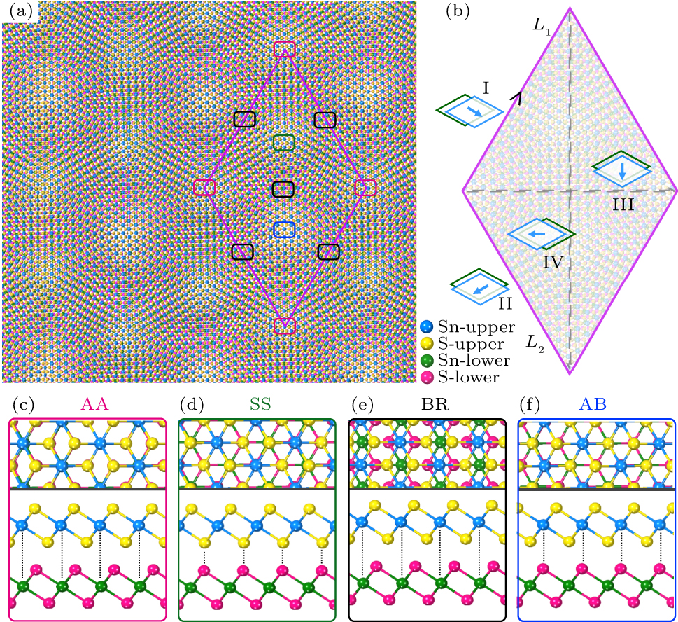
Through the analysis of the structure, we identify that the local interlayer stacking pattern in MSL regularly transfers with the position vector. For example, the local interlayer stacking patterns along four typical paths (path I–IV) reveal that the upper layer moves perpendicularly towards the path direction (Figs. 2(b) and
S1 ). We realize that, by extension, the local interlayer stacking patterns in MSL can be regarded as the regular movement of upper unit with respect to the lower unit. It is worthwhile mentioning that this rule is valid for all MSLs with a small twist angle. Here we adopt a 13 × 13 point mesh to slice the rhombus SnS2 MSL, for comparison, we separately computed the structures with fixed and variable interlayer distance (Fig. S2 ) and found that their bandgap variation trends are consistent, albeit to varying degrees. Based on prior research,[39] the formation of a spiral dislocation structure can effectively stabilize the lattice distance and transfer stress to the center of the spiral dislocation. In order to be consistent with experimental observation, the sliced local structures are set with a constant interlayer distance of 0.592 Å[66] and are fixed during the structure optimization. The small twist angles in all local stacking structures are treated as zero to satisfy the periodic boundary condition. This approximation is based on the expectation that the characteristics of local interlayer interactions are mainly determined by the local stacking patterns and are minimally affected by the small twist angle. According to this method, we have successfully verified the band gap reduction (∼ 0.6 eV) and the increase in carrier lifetime of spiral BiOCl MSL.[39] As shown in Fig. 2(c), we provide the atomic structures at four high symmetry regions, namely, AA, SS, BR, and AB structures, where AA structure is the ground-state stacking pattern of bulk SnS2, SS structure denotes the head-to-head arrangement of the S atoms from adjacent layers, the Sn-upper atom in BR structure locates on the bridge of two Sn-lower atoms, and the Sn-upper atom in AB structure locates on the top of the S-lower atom.To explore the evolution of interlayer interactions in SnS2 MSL, we performed DFT calculations on the electronic properties of local stacking patterns. As shown in Fig. 3(a) and
Table S1 , the spatially resolved band gap (Eg(r)) of SnS2 MSL shows strong dependence on position r (with a counterclockwise rotation of 90° with respect to the MSL in Fig. 2(b)), varying from the minimum 1.11 eV in the area around SS region to the maximum 1.51 eV of AA structure. Our calculations demonstrate a 0.40 eV band gap reduction of SnS2 upon the emergence of MSL. To confirm the suitability of GGA-PBE exchange–correlation, the HSE06 hybrid functional method was chosen for parallel comparison,[67] which returned a comparable band gap reduction of 0.37 eV. Furthermore, we separately aligned the energies of conduction band minimums (CBMs) and valence band maximums (VBMs) with respect to the corresponding vacuum levels for the 13 × 13 local stacking patterns of SnS2 MSL (seeFigs. S3(a) and S3(b) ), both of them exhibit the triple rotation symmetry similar to the spatially resolved band gap. The global minimums of CBM map and the global maximums of VBM map are both located in the same area around SS structure (seeTables S2 and S3 ), indicating the in-site transition of SnS2 MSL in real space. To confirm the accuracy, a large-scale first-principles calculation code[56] is recommended to make the comparison. The calculated charge distributions of CBM and VBM of bilayer SnS2 MSL with a 3.1° twist angle are shown inFigs. S3(c) and S3(d) , which are similar to the spatially resolved band-edge maps from our method. This similarity enhances the credibility of our simulations.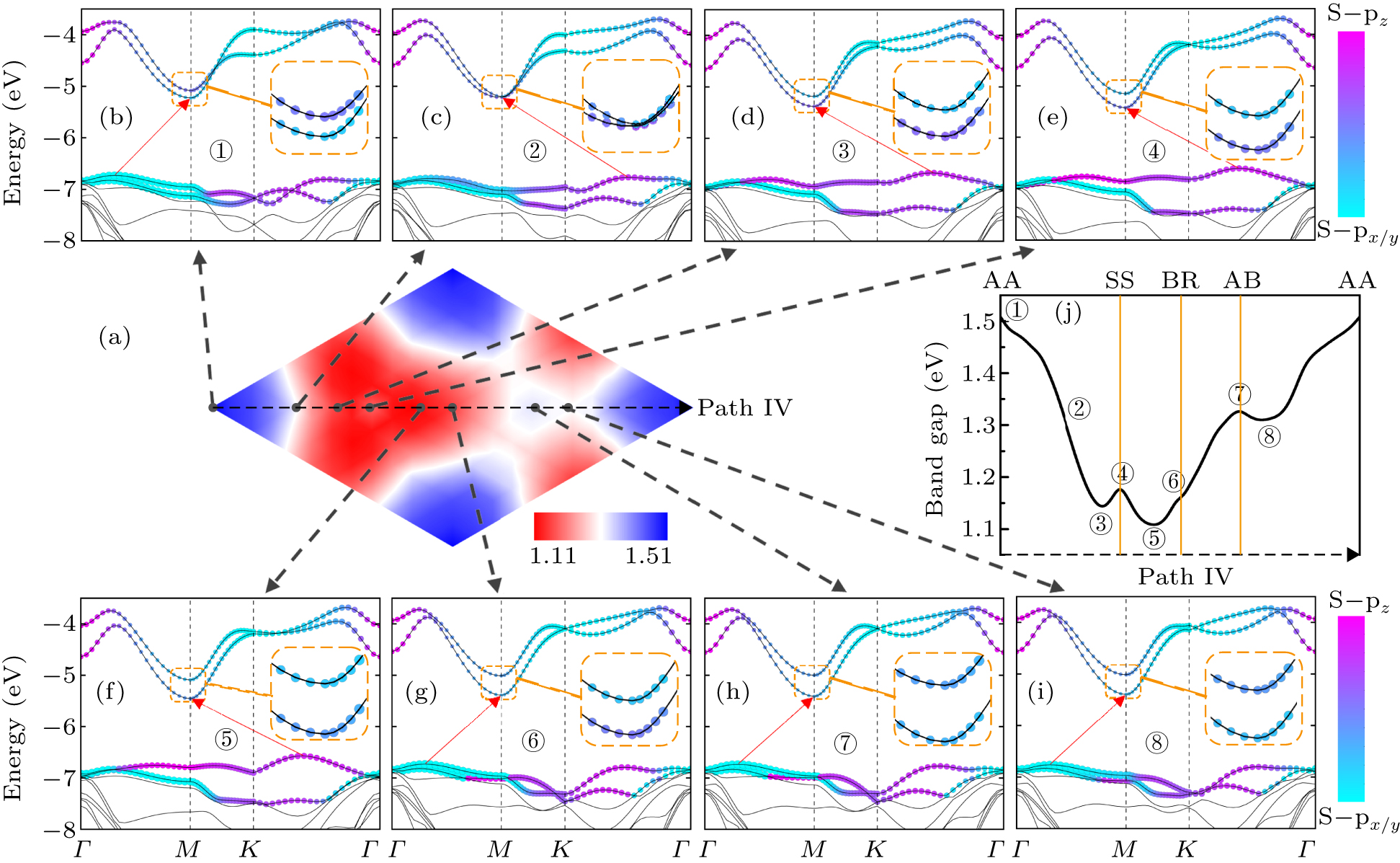
Because the four high-symmetry stacking patterns and the regions of band gap minimum/maximum are all located on path IV, we will take it as an example to explain the band gap reduction in SnS2 MSL. Figures 3(b)–3(i) illustrate the evolution of band structures of the local stacking patterns along path IV, and the corresponding evolution of band gaps is plotted in Fig. 3(j). For the convenience of comparison, their orbital energies are all aligned to the vacuum levels. We can see that the band structures of eight chosen stacking patterns all hold the indirect band gap transition character. Moreover, both CBM and VBM contribute to the band gap reduction in SnS2 MSL according to their evolutions as shown in
Fig. S4 . As the position vector moves along path IV, CBM always locates at M point, while the location of VBM first transfers from Γ–M path to Γ–K path accompanying with the band gap decrease to the global minimum, then it transfers back to Γ–M path with an increase in the band gap. To further understand this, the in-plane px/y orbital and the out-of-plane pz orbital of S atoms are projected separately for the four bands near the Fermi level. The close-up image in Fig. 3(b) shows that CBM and the second CBM of AA structure are mainly contributed by the in-plane px/y orbital and the out-of-plane pz orbital of S atoms, respectively. As the band gap decreases, the pz orbital descends faster than the px/y orbital and surpasses the latter to become the new CBM at position ②. Their energy difference reaches the maximum at position ⑤, which is also the stacking region where the band gap is the global minimum. Then the pz orbital gradually ascends and once again becomes the second CBM with the band gap increasing. To some extent, the situation of VBM is similar to that of CBM. It is mainly occupied by the in-plane px/y orbital concentrated at Γ–M path in AA structure, then at position ② the out-of-plane pz orbital concentrated at Γ–K path takes over the contribution to VBM until position ⑤. Soon afterwards, the VBM is occupied by the px/y orbital concentrated at Γ–M path and continues to the end. We conclude that both the downward shifting CBM and the upward shifting VBM in the area around SS structure are dominated by the pz orbital, which arises from the short distance of head-to-head arrangement of S atoms from adjacent layers. Furthermore, the relevant charge distributions of CBM and VBM for eight stacking structures along path IV are shown inFig. S5 , we can clearly see that the charges of VBM at position ③–⑤ are distributed along the out-of-plane direction. The locally enhanced interlayer interaction upon appearance of MSL is responsible for the large band gap reduction in SnS2 MSL.To probe the potential effects of distinct regions under different stacking patterns on optical activities of SnS2 MSL, we calculated the wave function overlap between VBM and CBM,
Table S4 ). Furthermore, we have also investigated the wave function overlap behavior for direct band gap transition (Fig. 4(b) andTable S5 ). It shows the enhanced overlap capability with respect to AA region, however, the mostly enhanced regions are around SS and AB structures. Strikingly, the distribution map of overlap integrals for direct band gap transition is consistent with that of spatially resolved band gap in real-space, which indicates the usability in optoelectronics.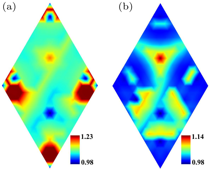
-
In conclusion, we propose that the MSL can be obtained through screw dislocation driven growth with a processing method to form a small twist angle, which provides more potential for the field of MSL materials. Taking SnS2 MSL as an example, we investigate its position-dependent electronic and optical properties. First-principles calculations show that the spatially resolved band gap exhibits a considerable reduction of 0.4 eV with respect to bilayer SnS2. According to the detailed analysis along the high symmetry path IV in the SnS2 MSL, we demonstrate that the considerable decrease/increase of CBM/VBM at regions around SS structure is dominated by the out-of-plane pz orbital, associating with locally enhanced interlayer interaction. On the other hand, the significantly enhanced optical activity of indirect/direct band gap transition in SnS2 MSL is verified by using the wave function overlap integrals method. Although our method cannot perfectly describe the structural characteristics, it is still qualitatively sufficient to guide the exploration of 2D MSLs.
The screw dislocation-driven MSL approach is expected to be expanded in transition metal dichalcogenides (TMDs) and other materials. Currently, spiral structures are experimentally synthesized mainly based on vapor deposition methods. For example, large-size 2D SnS2 crystals were prepared on mica sheets by screw-dislocation-driven (SDD), its possible mechanisms of generation and expansion were explained. The prepared photodetectors exhibited excellent photostability, reproducibility and optical response time.[46] Meanwhile, Madoune et al. investigated the growth mechanism of spiral pyramidal WS2 formed based on physical vapor deposition and its interesting optical properties using atomic force microscopy and Raman spectroscopy.[47] The first large-scale synthesis of spiral MoSe2 via flux-controlled chemical vapor deposition method was reported by Ahn et al., resulting in significant enhancement of the nonlinear optical signals attributed to the combination of broken inversion symmetry and exciton resonance effects.[48] These studies highlight the feasibility of employing spiral dislocation-driven methods to modulate MSL configurations in TMD materials. Nevertheless, deeper theoretical investigations are warranted to comprehend underlying structural mechanisms. Instructively, Ouyang et al. reviewed the structural evolution of spiral nanopyramids, spiral nanowires, etc., emphasizing the enhanced light–matter interactions and device physics.[49] While MSL represents a promising method for modulating TMDs, theoretical research in this area remains limited. Our proposed theoretical mechanisms for small-angle twisted MSL formed by spiral dislocations enrich theoretical frameworks, presenting new opportunities for optoelectronic devices and customized designs. Spiral dislocation-driven growth methods will be a potent means to expand the MSL family and diversify its applications.
 DownLoad: