
 首页
首页 登录
登录 注册
注册


HTML
-
Transmission electron microscopy (TEM) has long served as a foundational technique in materials science, enabling atomic-resolution investigation of material microstructures. This methodology provides crucial insights into atomic arrangements, chemical compositions, and electron configurations.[1–3] Scanning transmission electron microscopy (STEM), a powerful variant of TEM, further enhances its functionality by incorporating spectral imaging capabilities. This enhancement is achieved through systematic, point-by-point acquisition using a finely focused electron beam, facilitating detailed analyses of intricate local structural, chemical, and physical heterogeneities within materials.[4,5]
However, conventional imaging modalities employed in both TEM and STEM are typically optimized for static observations under standard vacuum conditions and ambient temperatures. This specificity restricts their applicability to materials exhibiting robust stability under electron beam irradiation, such as metals and metal oxides. The inherent limitations of these conventional methodologies frequently preclude their use for electron-beam-sensitive substances, including organic crystals, polymers, and organic–inorganic hybrid materials. Additionally, certain inorganic classes like hydrates and hydroxides are also susceptible to irreversible damage upon exposure to the electron beam.[6] Similarly, the utility of these conventional electron microscopy techniques in life science research is also limited. The high-dose and high-energy electrons necessary for imaging can induce the degradation of soft materials and biomaterials, posing significant challenges in preserving the integrity and intrinsic features of beam-sensitive samples during microscopic examination.
The advent of Cryo-TEM and its associated techniques has revolutionized structural research in the life sciences. This groundbreaking technology has offered unprecedented capabilities for high-resolution study of the microstructure of electron-beam-sensitive materials, overcoming the limitations of previous techniques.[7] It has significantly influenced our understanding of the fine structure of biomolecules, impacting fields such as drug design and disease mechanism research.[8,9] This impact was recognized by the award of the 2017 Nobel Prize in Chemistry. The key to Cryo-TEM’s success lies in its innovative method of rapidly freezing biological molecules into a hydrated vitreous state, enabling stable imaging using electron beams at low temperatures.[10] Additionally, automated data collection and single-particle reconstruction methods average the dose over a large number of identical particles and then algorithmically reconstruct the three-dimensional (3D) structural features of a single particle. Hardware advancements have also significantly enhanced Cryo-TEM performance. These include highly stable cryogenic sample stages, aberration correctors, and direct electron detectors.[11]
Recently, Cryo-TEM has extended its impact beyond life sciences, evolving into a powerful tool for exploring new phenomena in physics, chemistry, and engineering.[12–18] While the seeds of Cryo-TEM were sown in the physical science during the 1960s as low-temperature TEM,[19,20] the technique initially lacked widespread adoption due to limitations such as low spatial resolution and limited observation time caused by sample drift. The breakthrough of Cryo-TEM in structural biology has rekindled interest among physicists and materials scientists in its potential for condensed matter physics and materials science research.[21,22] Cryo-TEM’s stable low-temperature environment (around 77 K, the boiling point of liquid nitrogen), aberration-corrected electron optics, and low-dose imaging mode, coupled with advancements in single-particle Cryo-TEM data collection, have opened up exciting possibilities for unraveling the structural features of electron-beam-sensitive and quantum functional materials.
This review highlights emerging applications of Cryo-TEM in investigating the atomic structures of electron-beam-sensitive materials, particularly those containing organic components. We focus on recent advancements in revealing critical features for understanding quantum phenomena, including charge order and topological spin textures. By exploring the limitations of the current techniques, we identify key challenges and illuminate exciting future opportunities in this rapidly evolving field.
-
TEM utilizes high-energy electrons to probe the structure and composition of materials at the atomic level. Based on the conservation of kinetic energy in the collision system, this interaction results in scattered electrons, categorized as either elastic or inelastic scattering.[1] Elastic scattering, predominantly caused by Coulomb interactions between incident electrons and atomic nuclei within the specimen, deflects their trajectories by exchanging kinetic energy without altering their internal states.[6,23,24] While valuable for structural information, elastic scattering offers limited insight into chemical composition. In contrast, inelastic scattering involves the Coulomb interaction of incoming electrons with the atomic electrons surrounding each nucleus, altering their trajectory and losing energy. This energy transfer excites various phenomena within the material, such as plasmon oscillations, conduction or valence electron excitations, and direct ionization of inner atomic shells.[23,25–27] As shown in the diagram in Fig. 1(a), these excitations manifest as diverse signals, including secondary/Auger electrons, x-rays, cathodoluminescence, and heat. Notably, the energy imparted to the sample by imaging electrons often surpasses the material’s work function, resulting in the immediate ejection of electrons and the formation of free radicals and even broken bonds.[1]
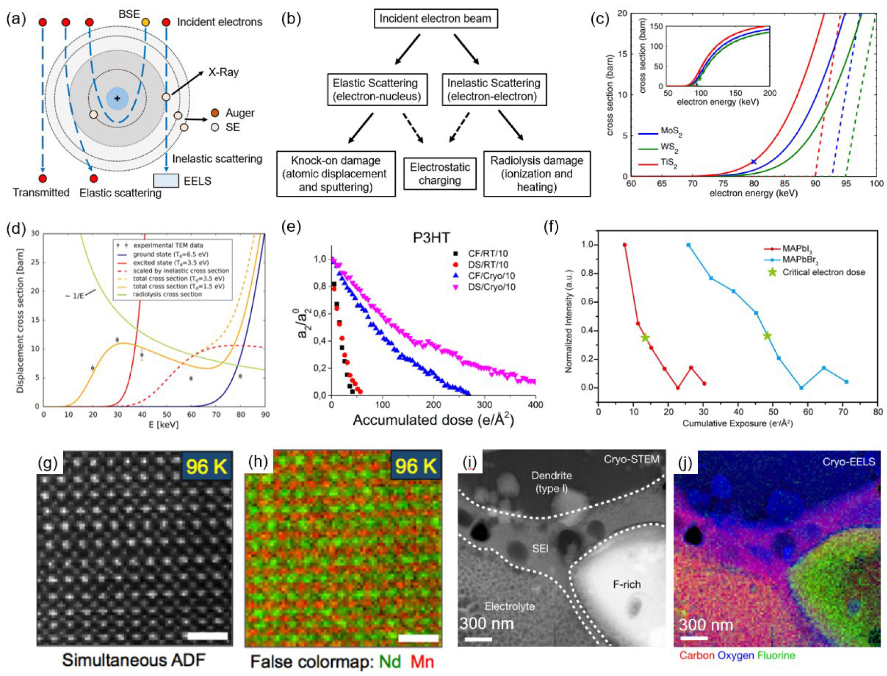
According to the mechanism of interaction between incident electrons and specimen, electron beam-induced damage primarily manifests in two forms: knock-on damage and radiolysis (Fig. 1(b)).[6,23] Knock-on damage, a direct consequence of elastic collisions between imaging electrons and atomic nuclei, occurs when high-energy electrons transfer momentum to an atom, causing it to be dislocated from its lattice position if the beam energy exceeds the atom’s displacement energy.[26,28] This threshold energy depends on the specific atom’s binding energy and atomic weight, and can be significantly reduced by pre-existing defects. Inorganic materials, particularly two-dimensional (2D) materials, are often more susceptible to knock-on damage. This can be effectively mitigated by reducing the imaging voltage of TEM. Studies have shown, for instance, that the displacement threshold for carbon atoms in graphene is 80 keV, while for sulfur atoms in monolayer MoS2 and WS2 it is 90 keV (Fig. 1(c)).[29–31] Knock-on damage can be avoided mainly by lowering the imaging voltage below these thresholds. However, recent research suggests that even at energies significantly lower than the knock-on threshold, the interplay between knock-on events and electronic excitations might still lead to vacancy formation, highlighting beam-induced damage’s complexity and nuanced nature (Fig. 1(d)).[32] Radiolysis, another primary form of electron beam-induced damage, stems from inelastic scattering interactions involving electron–electron or electron–phonon collisions.[23] These interactions generate long-lived electronic excitations that can trigger diverse processes within the material, such as ionization, heating, electrostatic charging, diffusion, and segregation.[23,28] The severity of radiolysis damage depends on the material’s ability to convert energy and momentum transferred during inelastic scattering.[25] Notably, when thermal vibrations facilitate this energy-momentum conversion, the Arrhenius law governs the rate of atomic jumps, highlighting the strong temperature dependence of radiolysis in such cases.[23,28,33]
TEM imaging involves both elastic and inelastic scattering, leading to the coexistence of knock-on and radiolysis damage.[23,34] Identifying the dominant mechanism for a specific material is crucial for selecting appropriate imaging conditions to minimize the structural degradation. For instance, 2D materials primarily experience knock-on damage, effectively mitigated by reducing the imaging voltage.[30,31,35–37] Conversely, ionic materials like transition metal oxides and fluorides are more susceptible to poor conductivity and accumulated charging. This can be alleviated by lowering the beam current to a specific dose rate.[38,39] Many dose-sensitive materials, including organic, organic–inorganic hybrid structures, polymers, zeolites, MOFs and COFs, exhibit radiolysis damage dependent on the cumulative electron dose and display distinct thresholds for structural degradation.[27,40–47] For instance, MOFs such as UiO-66 (Zr) and ZIF-8 (Zn) exhibit structural degradation at cumulative electron doses as low as 17 e−⋅Å−2 and 25 e−⋅Å−2, respectively, losing crystallinity entirely above 100 e−⋅Å−2.[48,49] Organic–inorganic hybrid perovskites display even greater electron beam sensitivity in room temperature conditions, with thresholds as low as a few electrons Å−2.[49] This vulnerability stems from the weak covalent bonds between organic ligands (e.g., HC(NH2)2, CH3NH3) and Pb atoms in perovskites. Even their inorganic counterparts, where Cs+ replaces organic ions, can only tolerate a few thousand electrons Å−2 at a dose rate of ≈ 100 e−⋅Å−2⋅s−1.[50,51] This limited tolerance to electron beam irradiation renders MOFs and organic–inorganic hybrid perovskites unsuitable for high-resolution imaging using conventional TEM techniques.
-
Given the strong temperature dependence of radiolysis, low-temperature imaging techniques like Cryo-TEM offer a powerful strategy to minimize damage and increase the critical dose of beam-sensitive materials.[52] This approach leverages the suppression of thermal vibrations, which influence energy transfer during beam-materials interactions.[53] This effect proves particularly beneficial for insulating materials like MOFs, where conventional high-resolution TEM (HRTEM) imaging often leads to complete amorphization.[48] Cryo-TEM, at liquid nitrogen temperatures, allows for the visualization of intricate pore structures within MOF-5 and reveals details like CO2 binding sites and lattice expansions within ZIF-8 frameworks.[54] Cryo-TEM extends beyond static observations, enabling dynamic investigation of beam-sensitive macromolecules with subsecond resolution. This approach allows visualization of self-assembly, nucleation, and growth processes without significant structural damage.[17,55–57] As shown in Figs. 1(e) and 1(f), studies have quantitatively demonstrated a significant enhancement in the irradiation durability of crystalline organic polymers and organic–inorganic hybrid perovskite materials under cryogenic conditions. Compared to ambient settings, the critical doses for these materials increase by up to 7-fold and 4-fold, respectively.[58,59] Additionally, given that the inevitable hydrocarbon contamination on the sample surface can induce electronic excitation (radiolysis damage),[23,32] low temperatures can also aid in preserving structure integrity for materials susceptible to knock-on damage. Namely, low-temperature environments can mitigate beam-induced structural damage in most specimens.
Innovations in modern electron detection technologies in Cryo-TEM also offer a significant advantage for the high-resolution structural investigation of electron beam-sensitive materials, which provides high signal-to-noise ratio (SNR) readouts under low-dose imaging conditions. Conventional TEM relies on scintillator-based charge-coupled device (CCD) cameras for real-time microstructure readout. To mitigate damage from direct exposure to high-energy electrons, CCD-based cameras employ a scintillator that converts the electron signal into photons. These photons are then relayed through optical fibers or lenses before being reconverted into electronic signals for readout.[60] However, this approach introduces several challenges. The scintillator can scatter electrons, and both optical fibers and lenses can scatter photons. Thus, during signal transmission, critical information is inevitably attenuated, and the point-spread function (PSF) broadens, leading to a reduction in SNR. Moreover, readout in CCD cameras involves a line-by-line charge transfer to a serial register, followed by pixel-by-pixel reading. This sequential readout mode inherently restricts the readout speed, limiting its effectiveness in precise motion correction of specimens.
In contrast to conventional TEM employing CCD cameras, Cryo-TEM equipped with direct-detection electron-counting (DDEC) cameras utilizes a more direct electron detection approach. DDEC cameras rely on electron counters, typically fabricated from semiconductors such as silicon or gallium arsenide, which generate a charge signal upon electron impact. This signal is then amplified and digitized. The DDEC camera’s array of electron counters builds a structural image by integrating the counts and energies of detected electrons. Such advanced architecture eliminates conversion and transmission noise, leading to a significant improvement in quantum detection efficiency. Due to the high sensitivity of DDEC cameras approaching single-electron detection and a wide dynamic range for detecting both high and low-intensity signals, modern Cryo-TEM allows for the definitive structural determination of biological materials, organic crystals, and hybrid materials, which are challenging for conventional TEM with CCD cameras.
Beyond its role as the primary camera in TEM mode for high-resolution imaging of electron beam-sensitive materials, the DDEC camera also excels in STEM mode for collecting electron energy loss spectroscopy (EELS) signals. Achieving atomic resolution in EELS elemental imaging requires significantly longer dwell times per pixel than conventional high-resolution annular dark field (ADF) atomic structure imaging. This poses a challenge for conventional scintillator-based indirect cameras, as extended exposure times (several seconds or more per atomic column) are needed to gather sufficient signals. Under cryogenic conditions facilitated by side-inserted Cryo-sample holders, inevitable sample drift further blurs the atomic-resolution chemical signal during such prolonged exposures. The DDEC camera overcomes this hurdle through its high quantum detection efficiency, significantly reducing the time required to collect spectral maps. For example, Lena et al. employed the Gatan K2 Summit DDEC camera for cryogenic EELS mapping, acquiring clear atomic-resolution elemental maps of 23 nm × 23 nm regions in just 13 s (Figs. 1(g) and 1(h)).[61] This remarkable feat underscores the synergistic potential of Cryo-STEM and DDEC cameras to advance our understanding of the spatial modulation of electronic states and nanoscale heterogeneity. Notably, near-atomic resolution analysis of bonding states in organic materials is still out of reach with current technologies. Even though low-temperature environments mitigate radiation damage, the electron dosage that organic materials can withstand is still significantly insufficient for DDEC cameras to acquire an adequate signal for detailed electronic structure analysis. Nonetheless, cryogenic low dose EELS continues to provide valuable insights for research on electron beam-sensitive materials. Examples of such contributions include elucidating elemental segregation at liquid/solid interfaces in battery materials (Figs. 1(i) and 1(j)), probing bonding environments and conjugation differences in soft polymers.[62–65]
-
The rapid development of low-dose imaging techniques for Cryo-TEM has been a boon for studying material systems containing organic components. Since the chemical composition of most organic materials is similar to that of biomolecules, they are highly susceptible to electron beam-induced radiolysis damage, which has long excluded these materials from conventional electron microscopy imaging. Crystal structure analysis is crucial for understanding crystalline materials’ physical and chemical properties. Traditional methods for resolving the crystal structure of materials with organic components typically involve using x-ray, neutron, or electron diffraction techniques in reciprocal space to determine the periodic structure of the crystal. This diffraction amplitude-based phase derivation has limitations in spatial resolution and is unable to handle polycrystalline and locally disordered structures. The powerful real-space high-resolution imaging capability of low-dose Cryo-TEM has become a solid complementary tool for studying structures of electron beam-sensitive materials alongside x-ray and neutron measurements.
Organic–inorganic halide perovskites have become a hot research topic in the photovoltaic field due to their excellent photovoltaic performance. They also exhibit promising applications in light-emitting diodes, ferroelectrics, and photodetectors.[66–70] Although many studies are devoted to improving their performance through control methods like minor doping, strain, grain boundaries, and structural distortion, the influence of these methods on the material microstructure still lacks direct atomic-scale observation.[71–73] Traditional methods for studying the structure of organic–inorganic hybrid perovskites were mainly based on low-magnification electron microscopy and diffraction analysis. For example, Rothmann et al. irradiated MAPbI3 single crystals with a low-dose-rate (∼ 2 e−⋅Å−2⋅s−1) electron beam and monitored their decomposition pathway in real time using in situ selected area electron diffraction (SAED) technology.[74] The study revealed the decomposition pathway of MAPbI3 under electron beam irradiation. At the initial stage of exposure, MAPbI3 releases a small amount of ammonia (NH3) and hydrogen iodide (HI) molecules, leading to relaxation of the crystal structure, manifested as a decrease in the a-axis and c-axis parameters of the tetragonal lattice. With continued irradiation, NH3 and HI are further lost while the PbI6 octahedron relaxes and tilts or rotates, and additional forbidden reflection peaks appear in the diffraction pattern. With increasing irradiation, the additional forbidden reflection peaks eventually disappear, and the remaining diffraction peaks broaden, indicating that the crystal structure is severely damaged and the long-range ordered crystal lattice period is lost. Their study also showed that the decomposition rate of MAPbI3 mainly depends on the total irradiation dose and has little relationship with the irradiation rate.
Chen et al. used a lower dose rate (1e−⋅Å−2⋅s−1) electron beam irradiation and observed a similar decomposition process by continuous SAED.[75] They found that the diffraction pattern matches the simulated tetragonal MAPbI3 crystal structure in the early irradiation stage. With the progress of irradiation, the intermediate phase MAPbI2.5 appears, and its formation is attributed to the generation of halogen ion vacancies and local ordering of the remaining halide ions. Finally, the perovskite structural framework collapses to form a layered PbI2 structure. Different from the research of Rothmann et al., Chen et al. found that the irradiation rate also affects the decomposition rate, with a higher rate accelerating the decomposition of MAPbI3. However, electron diffraction analysis alone cannot directly confirm their speculation on the structural changes. Using a low-dose DDEC camera, Chen et al. directly observed that ordered organic cation (MA+) vacancies appeared before I− ion vacancies.[76] Therefore, the superstructure diffraction spots in the diffraction pattern may come from the ordered cation vacancy of MA0.5PbI3. Based on calculation analysis, Cai et al. believed that under the irradiation of a 300 kV high-energy electron beam, the loss of MA and iodine in MAPbI3 coincides, rather than in a sequential decomposition.[77] This is because the kinetic energy provided by the high-energy electron beam irradiation exceeds the energy required to knock atoms out of their positions, resulting in simultaneous bond breaking. However, such analysis based on knock-on damage may not apply to organic–inorganic hybrid perovskite crystals because these materials decompose more readily due to the ionizing effects of radiation. Subsequent studies have shown that, surprisingly, higher acceleration voltages increased the dose required to induce significant decomposition of hybrid organic–inorganic perovskites.[78] This finding indicates that the degradation mechanism for organic–inorganic hybrid perovskites is primarily radiolysis rather than knock-on damage. Since high voltages facilitate a more efficient passage of electrons through the sample, minimizing their interaction time and reducing radiolytic damage.
The mechanism by which organic–inorganic hybrid lattices decompose under electron beam irradiation is a topic of ongoing debate. Researchers question whether halogen anions or organic cations are more readily removed from the lattice or if both depart simultaneously. This controversy stems from limitations in conventional methods. SAED cannot directly image atoms, relying instead on diffraction patterns to infer structural changes. However, interpreting these patterns can be ambiguous, leading to disagreements about the specific decomposition process. For example, additional peaks might be interpreted as new phases or artifacts from damage. Furthermore, hybrid perovskites have a low tolerance for electron dose. Even advanced techniques like DDEC cameras struggle to resolve the short-lived intermediate structures that form during structural transformation. Additionally, organic molecules are less visible in HRTEM images than inorganic components, which can lead to artifacts caused by electron beam damage being misinterpreted as organic molecules. Due to the predominance of radiolysis damage in electron beam-induced decomposition of hybrid materials, Cryo-TEM offers a significant advantage for revealing their intrinsic structural features by minimizing artifacts arising from beam damage during analysis. Cryo-TEM achieves this through two primary mechanisms. First, rapidly freezing the sample preserves its native state and suppresses chemical reactions that would otherwise generate volatile species such as NH3 and HI. Second, the low-temperature environment provided by liquid nitrogen reduces molecular thermal vibrations, thereby mitigating structural damage caused by electron beam heating.
In a recent study by Zhu et al., Cryo-TEM was employed to investigate the electron-beam-sensitive hybrid perovskite MAPbI3.[46] To minimize moisture exposure during sample preparation, the authors developed a low-temperature TEM sample transfer method detailed in Fig. 2(a). Large MAPbI3 crystals were initially ground into nanoparticles within an inert glovebox environment before being transferred onto a TEM grid. The sample was then promptly quenched in liquid nitrogen and transferred to the Titan Krios Cryo-TEM using a Cryo-loader to maintain a cryogenic temperature of (−190 °C) throughout the process. HRTEM imaging was performed at 300 kV using a DDEC camera. Notably, the MAPbI3 material exhibited a high density of (002)T-oriented stacking faults, as revealed by HRTEM (Fig. 2(c)), compared to the pristine atomic structure depicted in Fig. 2(b). These stacking faults are characterized by the presence of an additional MAI layer, and the cumulative electron dose of the sample in Fig. 2(c) is 94 e−⋅Å−2. Since no significant changes in the FFT pattern were observed, the authors suggest that the MAI-MAI stacking faults seen at this dose may represent an intrinsic plane defect in the MAPbI3 structure, potentially overlooked in previous studies. However, the presence of stacked dislocations does not necessarily alter the FFT pattern. Consequently, the consistency of the FFT pattern before and after irradiation cannot conclusively verify the structural integrity of MAPbI3 post-electron exposure. Additionally, with 94 e−⋅Å−2 exceeding the typical threshold for structural damage in most organic–inorganic hybrid perovskites, it is probable that MAI-MAI stacking faults arise as intermediate structures following organic molecule damage, rather than being inherent to the MAPbI3 structure. Employing first-principles calculations, the authors further revealed that while these stacking faults may hinder light absorption, the additional MAI layer can function as a micro-interface, promoting charge separation and reducing electron–hole recombination rates. This phenomenon holds theoretical promise for enhancing solar cell performance. In a study by Li et al., Cryo-TEM was employed to investigate the intrinsic atomic structure and degradation mechanisms of the perovskite solar cell material MAPbX3.[59] The authors defined the critical electron dose as the dose causing a diffraction peak’s intensity to decay to 1/e of its maximum value, analyzed by monitoring continuous changes in the FFT pattern under varying electron beam irradiation. They measured a critical electron dose of 12 e−⋅Å−2 for MAPbI3. Interestingly, the critical dose for MAPbBr3 under cryo-conditions was significantly higher at 46 e−⋅Å−2, representing a four-fold increase compared to the room temperature value of 11 e−⋅Å−2. At doses below this critical threshold, both MAPbBr3 and MAPbI3 retained their intrinsic atomic structures with a high spatial resolution of 1.49 Å, allowing visualization of individual [PbX6]4− octahedra and MA+ organic cations (Fig. 2(d)).
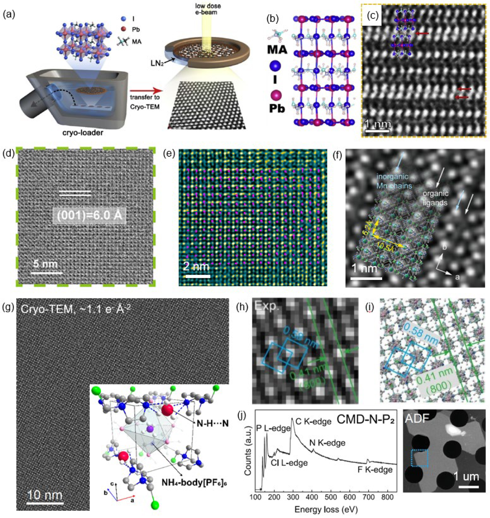
Benefiting from continuous advancements in Cryo-TEM imaging technology, the achievable resolution for the intrinsic atomic structure of MAPbI3 has been further improved, enabling observations at a lower accumulated electron dose of 5.96 e−⋅Å−2 (Fig. 2(e)). This technique even holds promise for quantifying the polarization offset of the methylammonium (MA) cations based on the ideal position of the tetrahedral center, akin to methods employed for inorganic ferroelectric perovskite materials.[79] Our collaborators, led by Loh, synthesized three Mn-based hybrid perovskite single crystals with varying dimensionality by modifying the organic component within the organic–inorganic hybrid perovskite structure.[80] These materials consisted of a 2D material, (4-fluorobenzylamine (FB))2MnCl4, a one-dimensional (1D) ((R)-3-fluoropyrrolidinium (FP))MnCl3, and a zero-dimensional (0D) (pyridine (PD))2MnCl4. Continuous-wave electron spin resonance (ESR) measurements were employed to investigate the correlation between the spin decoherence process and the crystal dimensionality. The results revealed that a rigid inorganic framework promotes a prolonged spin decoherence time. Compared to MAPbI3 and MAPbBr3, the Mn-based hybrid crystals exhibited a lower tolerance to electron beam irradiation. Even under cryogenic conditions (77 K), the critical threshold dose for the 2D (FB)2MnCl4 crystal did not surpass 5 e−⋅Å−2. As illustrated in Fig. 2(f), by utilizing a low-dose DDEC camera with a cumulative dose of 2.5 e−⋅Å−2, we successfully resolved the alternating chain structure formed by the Mn–Cl atomic columns and the misalignment of the interlayer Mn–Cl octahedra. Additionally, the organic ligands situated between the inorganic Mn chains were clearly visualized (indicated by white arrows). Cryo-EELS further corroborated the homogeneous distribution of various elements within the 2D (FB)2MnCl4 crystal.
Electron diffraction and HRTEM have been instrumental in elucidating structural complexities within inorganic perovskites and organic–inorganic hybrid perovskites, including ion polarization, structural distortions, vacancies, and grain boundary defects.[47,76,79,81,82] However, research on the crystal structures of all-organic perovskites, which lack metal cations, remains comparatively limited due to the challenges associated with both synthesis and characterization. The primary challenge in synthesizing all-organic perovskites stems from the substantial size difference between organic molecules and inorganic ions within the traditional ABX3 perovskite structure.[83] The larger size of organic molecules can induce steric hindrance between A-site and B-site cations, hindering the formation of stable structures. Consequently, only a limited number of organic molecules can be successfully integrated into perovskite structures. A significant advancement occurred in 2002 with identifying the dicationic piperazinium family of organic perovskites incorporating Cl−, Br−, and I− anions.[84] Subsequently, Xiong et al. further expanded the repertoire of 3D organic perovskites by incorporating various diammonium cations into their design.[85] However, the realization of 2D all-organic perovskites remained elusive until recent progress. In a recent breakthrough published in Science, our collaborators, Choi et al., proposed a novel strategy for synthesizing 2D all-organic perovskites.[86] Their method deviates from the traditional perovskite structure by introducing an additional cation and achieving a chemical formula of ABX2. This innovation creates a highly stable 2D configuration through a network of hydrogen bonds. The study further demonstrates the versatility of this approach by generating a range of 2D perovskites using different organic cations. Notably, these materials exhibit promising properties for use as flexible dielectric layers, as evidenced by field-effect transistor measurements. This research paves the way for the development of novel materials for future flexible electronic devices.
A critical gap exists in prior research on 3D organic perovskites, primarily relying on x-ray diffraction (XRD) for structural characterization. Limited transmission electron microscopy (TEM) use for real-space analysis arises from the high electron-beam sensitivity of all-organic perovskites. This sensitivity stems from the combined absence of metal cations and the dominance of hydrogen bonding in their structures, posing a significant challenge for low-dose TEM imaging techniques. For HRTEM analysis, we prepared few-layer 2D all-organic perovskite crystals using solution evaporation recrystallization. This method resulted in thin film samples that facilitated alignment with the desired crystallographic zone axis, which minimized electron beam exposure during zone axis identification. We employed a DDEC camera for sample navigation and target area selection at low magnification using the EPU and Velox software suite, ensuring that the total electron dose remained below 0.1 e−⋅Å−2. To achieve high-resolution imaging with minimal structural damage, over 30 high-magnification images were acquired subsequently at a dose rate of 0.1 e−⋅Å−2 per frame. Individual image analysis revealed a critical electron dose threshold of only 1.5 e−⋅Å−2 for complete structural degradation of the 2D organic perovskite. After removing structurally compromised frames, the remaining images were subjected to amplitude filtering, alignment, and stacking. To further enhance the SNR, a 3D stacking Wiener filter was applied to the final image stack.[84] This approach enabled near-atomic-resolution direct imaging of the 2D all-organic crystals at an ultra-low dose of approximately 1.1 e−⋅Å−2. As depicted in Fig. 2(g), each bright spot corresponds to an organic group assembled through covalent bonds. Driven by hydrogen bonding interactions, these organic groups arrange themselves into a perfect cubic all-organic 2D perovskite single crystal structure. The magnified HRTEM image in Fig. 2(h) is consistent with the atomic structure model refined using XRD data presented in Fig. 2(i). Additionally, we used Cryo-EELS to confirm the elemental composition and uniform distribution of various elements within the 2D all-organic perovskite structure (Fig. 2(j)).
We identify a critical gap in prior research, which primarily relied on x-ray diffraction (XRD) to elucidate the structural characteristics of 3D organic perovskites. The limited use of TEM for real-space characterization can be attributed to two main factors. First, the field of organic perovskite research is still in its early stages of development. Notably, the absence of metal cations renders these all-organic materials inherently susceptible to damage under electron beam irradiation. Additionally, the hydrogen bonds, crucial for the assembly of organic molecules into long chains within the perovskite framework, are highly sensitive to electron beam exposure. Consequently, HRTEM studies of all-organic perovskite structures pose a significant challenge for low-dose TEM imaging. To facilitate HRTEM analysis, we prepared few-layered 2D all-organic perovskite crystals via solution evaporation recrystallization. This approach yielded thin film samples that enhanced the probability of encountering the desired crystallographic zone axis, consequently minimizing electron beam exposure during zone axis identification. Utilizing the EPU and Velox software suite, we employed a DDEC camera for sample navigation and target area selection at low magnification, and ensured the total electron dose remained below 0.1 e−⋅Å−2. To achieve high-resolution imaging with minimal structural damage, over 30 high-magnification images were subsequently acquired at a dose rate of 0.1 e−⋅Å−2 per frame. Individual image analysis revealed a critical electron dose threshold of only 1.5 e−⋅Å−2 for complete structural degradation of the 2D organic perovskite. Following the removal of structurally compromised frames, the remaining images were subjected to amplitude filtering, alignment, and stacking. To further enhance the SNR, a 3D stacking Wiener filter was applied to the final image stack. This approach enabled near-atomic-resolution direct imaging of the 2D all-organic crystals at an ultra-low dose of approximately 1.1 e−⋅Å−2. As depicted in Fig. 2(g), each bright spot corresponds to an organic group assembled through covalent bonds. Driven by hydrogen bonding interactions, these organic groups arrange themselves into a perfect cubic all-organic 2D perovskite single crystal structure. The magnified HRTEM image in Fig. 2(h) is consistent with the atomic structure model refined using XRD data presented in Fig. 2(i). Additionally, we used Cryo-EELS to confirm the elemental composition and uniform distribution of various elements within the 2D all-organic perovskite structure.
-
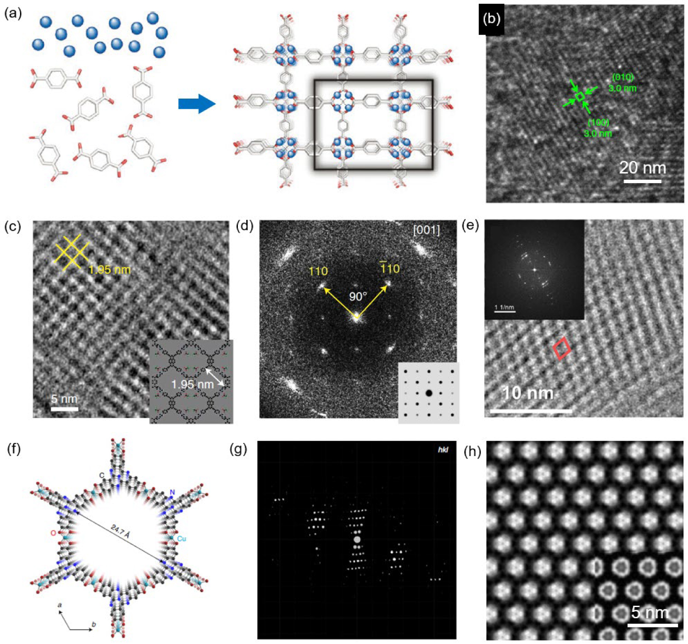
Metal–organic frameworks (MOFs) are constructed by assembling metal ions or clusters with organic ligands via coordination bonds. Covalent organic frameworks (COFs), on the other hand, are formed by the covalent linkage of conjugated organic molecules. These two types of porous materials have attracted significant research interest in recent years.[88,89] Using metal ions/clusters and organic molecules as building blocks and employing a bottom-up assembly approach, MOFs and COFs exhibit remarkable advantages in designable and tailorable molecular functionalities, porosity, and well-defined topological structures. The molecular functionalities originate directly from the constituent building blocks, while the topological functionalities arise from the periodic organic network and inherent porosity (Fig. 3(a)).[90] Diffraction techniques currently serve as the primary method for characterizing the periodic crystal structures of these two types of porous materials. However, the local non-periodic structures of MOFs and COFs, including crystal surfaces, boundaries/interfaces, guest molecules, and point/extended defects, also significantly influence their properties, such as mass transport, adsorption, and catalysis.[91,92] For example, defects and interfaces play a critical role in the performance of MOF membranes for gas separation.[91] Unfortunately, probing the local structures of MOF crystals at high spatial resolution remains challenging due to organic components, which are sensitive to electron beam irradiation. This sensitivity has long excluded MOFs from conventional TEM imaging.[93,94] Indeed, high-resolution imaging of electron-beam-sensitive materials, including organic-incorporated perovskites, MOFs, and COFs, represents one of the most significant challenges in TEM characterization.[6,49] Developing new techniques for high-resolution imaging of such materials is a critical and urgent task in materials science and electron microscopy. Addressing this challenge would significantly advance the understanding of structure–property relationships in porous materials.
Low-dose HRTEM is a common approach to capture the intrinsic structure of porous materials before damage occurs.[48] A critical prerequisite for high-resolution structural characterization of these materials is determining the respective threshold doses for various MOF and COF materials. This knowledge enables the investigation of their intrinsic structures under non-damaging dose conditions. Early studies investigated the stability of ZIF-8 under a 300 kV electron beam by monitoring its electron diffraction patterns. They found that ZIF-8 began to lose crystallinity when the accumulated electron dose reached approximately 25 e−⋅Å−2. Subsequent research revealed that the stability of MOFs varies depending on the type and number of coordination bonds, as well as the material’s structure, composition, crystal size, and crystal orientation[48,54]. MOFs’ tolerable threshold electron dose ranges from a few to a few dozen e−⋅Å−2. Similar to MOFs, the stability of COFs, which are connected by covalent bonds, is influenced by various factors. Notably, the presence of π–π stacking interactions between ligands enhances COF stability. The tolerable electron dose for COFs ranges from a few to hundreds of e−⋅Å−2. These values define the maximum electron dose applicable during HRTEM imaging, which is approximately two to three orders of magnitude lower than those typically employed in conventional HRTEM. Such low doses correspond to only a few electrons per pixel at the magnifications required for atomic-resolution images. Conventional CCD cameras are unsuitable for these conditions because they require hundreds of electrons per pixel for an acceptable SNR. The low SNR explains the limited resolution observed in early attempts to image MOFs using HRTEM, even under cryogenic conditions (Fig. 3(b)).[95] The lowest doses used in conventional HRTEM still significantly exceed the damage threshold dose for MOFs, leading to framework structure destruction and the loss of high-frequency information in the resulting images.
The emergence of DDEC cameras and their application have revolutionized the structural characterization of porous materials. Notably, the electron-counting functionality of these cameras allows for the capture of structural information at ultra-low doses (10−2e−⋅pixel−1). Their exceptional detection efficiency enables HRTEM imaging at sufficiently low electron beam doses, thereby preserving the integrity of sensitive materials. Remarkably, for some less-sensitive MOFs and COFs, atomic-resolution TEM images can be obtained even at room temperature using DDEC cameras.[49,96] The combined application of Cryo-TEM and DDEC cameras has facilitated the investigation of the intrinsic pore structure of COFs. For instance, we exfoliated imidazopyridinium-linked COF (IP-COF) using ethanol-assisted liquid ultrasonic dispersion. The resulting thin sheets were dispersed onto Quantifoil carbon grids and frozen at liquid nitrogen temperature (approximately 77 K) for HRTEM analysis.[97] Ultrasonication typically led to random stacking of the IP-COF sheets. The random stacking resulted in sharp first-order characteristic diffraction rings in the FFT patterns of the high-resolution structures of multilayer regions, which corresponded to the (110) lattice periodicity of IP-COF. During high-resolution structural characterization, the random stacking of COF layers created moiré patterns, hindering the direct resolve of the intrinsic pore structural features of the material. By leveraging the large-area sample search function provided by EPU software, we efficiently located unrotated, few-layer IP-COF thin sheets under low electron dose exposure. Figure 3(c) presents a high-resolution lattice fringe image of a single, unrotated IP-COF-2 thin sheet recorded along the [001] zone axis. The image resolves the square pore structure with a side length of 1.95 nm, formed by interlaced carbon chains. This observation is consistent with the inserted IP-COF atomic structure model. The FFT pattern in Fig. 3(d) exhibits higher-order lattice periodicities, which matched the simulated reciprocal lattice obtained using the IP-COF atomic model. Additionally, AB-stacked IP-COF thin sheets were observed. The overlapping pore size in these structures is half that of the AA-stacked IP-COF pore size. The strong electron tolerance exhibited by IP-COF, with no apparent loss of crystallinity observed under a high dose of 100 e−⋅Å−2, can be attributed to abundant stable carbon-sulfur and ionic bonds. From its high sulfur content and structural stability, IP-COF is a promising candidate cathode material for lithium-sulfur batteries. When prepared with a high sulfur loading, the resulting lithium-sulfur batteries exhibit excellent areal capacity. Furthermore, IP-COFs demonstrate significantly improved sulfur redox chemistry, achieving a rate performance of 540 mAh⋅g−1 at 10 C.
MOFs, similar to COFs, possess networks of porous structures with dispersed metal ions/clusters. These metal centers exhibit a variety of metal-directed functionalities in applications like gas adsorption, drug delivery, catalysis, and energy storage. However, the weak coordination bonds in MOFs limit their stability and hinder their practical use. The Loh group has addressed this challenge by synthesizing a metal COF (pdiCOF-Zn) using Zn2+ ions as a template.[98] This approach achieves a crystallinity of approximately 1:1 ([Zn2+]:ligand), effectively combining covalently linked COFs’ stability with MOFs’ metal-directed functionalities, representing an innovative new material framework. We employed Cryo-TEM to acquire a high-resolution lattice fringe image of pdiCOF-Zn in a direction slightly tilted from the c-axis. As shown in the HRTEM image of Fig. 3(e), the rhombic pore pattern (indicated by the red box) is clearly resolved. The inserted FFT analysis confirms the periodicity of the observed real-space structure, demonstrating its consistency with the refined structure obtained from XRD. Additionally, low-dose ADF-STEM was used to visualize the triangular periodic distribution of Zn atoms in a direction slightly off the c-axis.
Cryo-TEM offers advantages over conventional TEM, including high mechanical stability and minimal sample damage. However, limitations exist. The integrated sample stage design effectively dampens external thermal vibrations but lacks dual-tilt functionality, restricting α-axis tilting to a ±70° range. Consequently, high-resolution material studies require thin-layer samples, as thicker specimens are more prone to intractable off-axis issues. To address this limitation, researchers have developed low-dose 3D electron diffraction (3DED) technology compatible with Cryo-TEM.[100–102] Combined with Cryo-HRTEM, this technique facilitates the analysis of the fine structure of microporous materials, particularly small-sized MOFs and COFs. Obtaining sufficiently large (>5 μm) and long-range ordered MOF/COF crystals for single-crystal XRD analysis can be challenging due to the interplay between nucleation and crystal growth processes. Therefore, traditional methods for structural analysis of many tiny, porous crystals rely on powder x-ray diffraction (PXRD) and pattern matching with hypothetical models. While PXRD provides basic structural information, it often lacks definitive evidence for fine structural features, such as the stacking order of material layers or pore content. Combining Cryo-TEM with low-dose 3DED technology enables the observation of nanoscale single-crystal particle samples. This technique continuously tilts the crystal sample around the goniometer axis to acquire a series of electron diffraction images. The images are then used to reconstruct the 3D reciprocal lattices. The resulting 3DED data can be analyzed similarly to single-crystal XRD data to elucidate the fine structure of the sample. Dou et al. exemplified this approach by synthesizing tiny single crystals of 2D π-conjugated Cu3HHTT2 MOFs. CuSO4⋅5H2O served as the metal source, while a solution of 2,3,7,8,12,13-hexahydroxytetraazanaphthotetraphene (HHTT) acted as the organic ligand.[99] Under cryogenic conditions, they employed 3DED technology with a resolution of ∼ 1.5 Å to investigate the fine structure of Cu3HHTT2. This analysis revealed that Cu2+ ions on adjacent HHTT cores coordinate with two neighboring catechol groups to form square [CuO4] secondary building units (SBUs). Each triangular HHTT ligand is coordinated by three of these SBUs, leading to the formation of infinite, planar 2D layers (Figs. 3(f)–3(h)). Furthermore, cRED confirmed that these layers adopt a fully eclipsed AA stacking arrangement. The combined application of cRED with Cryo-HRTEM revealed an extended honeycomb structure with well-aligned pores exhibiting a diameter of 2.3 nm.
Beyond high-resolution imaging of the sensitive pore structures, Cryo-TEM facilitates ex-situ and operando investigations, enabling the study of the fine structure of porous materials after guest molecule adsorption and the real-time process of single-crystal structure assembly from amorphous precursors. Cui et al. developed a Cryo-TEM sample preparation method involving extended CO2 exposure of ZIF-8 crystals, followed by rapid quenching in liquid nitrogen to inhibit gas desorption.[54] The CO2-filled ZIF-8 crystals were then subjected to atomic-scale structural analysis using Cryo-TEM. Initially, the electron dose tolerance of ZIF-8 was evaluated at room and low temperatures. Exposure to ∼ 25 e−⋅Å−2 at room temperature resulted in rapid, significant structural damage to the ZIF-8 particles. Complete loss of crystallinity was observed upon reaching a cumulative electron dose of 50 e−⋅Å−2. HRTEM images and FFT patterns confirmed the amorphization of the material. Conversely, ZIF-8 exposed to 90 e−⋅Å−2 at low temperature exhibited only partial loss of crystallinity. Using high-resolution imaging below the damage threshold, the researchers compared the crystal structures of empty and CO2-filled ZIF-8 crystals at atomic resolution (1.86 Å). Figures 4(a) and 4(b) show contrast transfer function corrected HRTEM images of empty and CO2-filled ZIF-8, respectively. Brighter regions indicate higher density. Zinc clusters (bright spots) form a hexagonal lattice. Notably, the void centers (marked by blue circles) differed between the two states. In the empty state, the void appears dark, while in the CO2-filled state, a bright center suggests adsorbed CO2. Additionally, the filled state exhibited a 3% lattice expansion. Figure 4(c) shows the corresponding atomic structure model obtained from density functional theory (DFT) calculations. To confirm the structure, the researchers examined crystals from another direction ([001] zone axis). Here, ZIF-8 particles appear square with two cavities (green circles and orange boxes in Fig. 4(d)). In the empty state (Fig. 4(d)), no contrast is seen in the cavities. Conversely, the CO2-filled state (Fig. 4(e)) shows bright contrast within the cavities. Consistent with the previous view, the (002) plane showed a 3% lattice expansion. These experiments demonstrate that Cryo-TEM enables stable imaging of ZIF-8, revealing its atomic structure and guest molecule interactions. However, the contrast in HRTEM images is modulated by the contrast transfer function (CTF), meaning that the image details may not align directly with the crystal structure without accurate CTF correction. Although the author can observe some bright contrast inside the cavities, they are unable to resolve individual Zn columns, indicating insufficient resolution or imperfect CTF correction, which may introduce artifacts. Therefore, additional evidence is required in this study to definitively link the contrast within the cavities to CO2 molecules. For example, exploring the use of low-dose electron irradiation to prompt CO2 desorption, followed by observing resulting structures at the same location, could provide insight. Additionally, examining CO2 molecule adsorption structures using alternative techniques like low-temperature XRD or STM may offer further clarity.
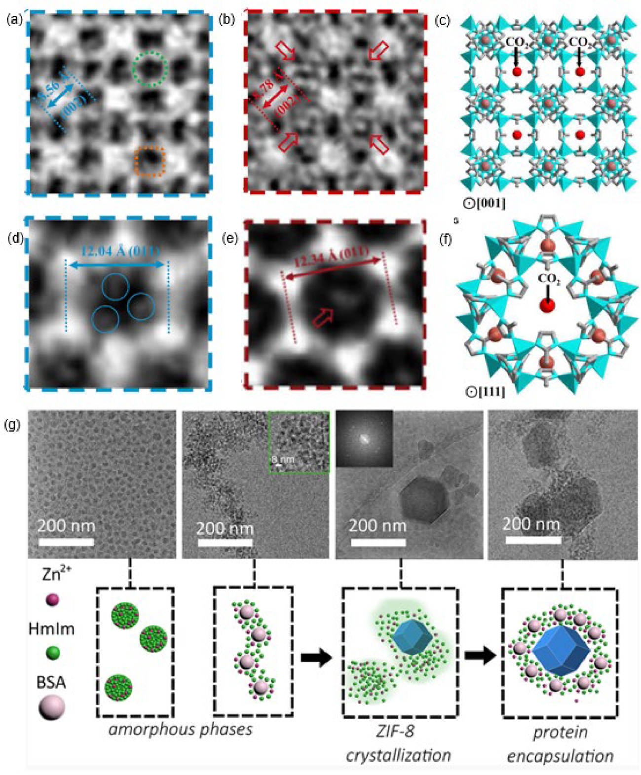
More recently, Alana and coworkers first prepared vitrified precursor samples by absorbing a solution of bovine serum albumin (BSA) and zeolitic imidazolate framework 8 (ZIF-8) precursors on TEM grids.[103] Subsequently, they vitrified the precursor sample using liquid propane quenching. Using time-resolved Cryo-TEM, they monitored the crucial role of proteins in the nucleation and growth processes of the amorphous precursors under low-dose electron irradiation. They discovered two vital amorphous phases: (i) 2-methylimidazole/zinc (HmIm/Zn) amorphous particles and (ii) protein/HmIm/Zn particles during the nucleation and growth. Furthermore, they identified two distinct growth mechanisms that depend on the ligand-to-metal precursor ratio. The ratio of ligand (HmIm) to metal (Zn) plays a key role in ZIF-8 crystallization. At high ratios (around 35:1), amorphous particles form first. These particles then dissolve and recrystallize into solid ZIF-8 (sodalite) through a non-classical process. This involves an initial, supersaturated amorphous phase that triggers the formation of ZIF-8 crystals. When a protein called BSA is present, it interacts with the ZIF-8 precursors, forming large protein-based particles. These BSA particles co-crystallize with ZIF-8, resulting in a BSA-ZIF-8 composite. At lower HmIm:Zn ratios (around 4:1) and without BSA, the amorphous particles don’t undergo the dissolution-recrystallization step. Instead, a different mechanism leads to the formation of a different ZIF-8 structure (diamondoid). However, BSA can still influence the process. By binding precursor ions, it creates local areas of high concentration, promoting the formation of sodalite ZIF-8 crystals around the protein particles. These crystals then grow to incorporate the BSA, resulting in BSA-ZIF-8 with nanopores. Figures 4(g) and 4(h) illustrate the Cryo-TEM images and corresponding schematics of the critical steps of these crystallization processes. By comparing the formation mechanisms of ZIF-8 and BSA-ZIF-8 systems through in situ observation by Cryo-TEM, the authors demonstrate the importance of transient amorphous phases in the design of protein–MOF structures and showcase the value of Cryo-TEM in the development of bio-based materials.
2.1. Mechanisms of electron beam damage
2.2. Advantages of Cryo-TEM for electron-beam-sensitive materials
2.3. Organic–inorganic hybrid and all organic perovskite
2.4. Porous materials
-
Quantum materials exhibit various exotic phenomena, including superconductivity, charge density wave (CDW), skyrmions, magnetic spin ice, and topological behavior. These phenomena emerge from intricate couplings between various order parameters, including charge, magnetism, orbital order, and lattice symmetry.[104] The material structure and properties frequently display spatial inhomogeneity across atomic to mesoscopic length scales.[105] A critical challenge in elucidating the intricacies of these materials lies in developing sophisticated probing techniques capable of capturing order parameters over multiple length scales, encompassing both local atomic environments and extended structural features. However, the manifestation of many quantum phenomena is confined to low-temperature regimes, posing a significant hurdle to the thermal stability of conventional characterization tools.
Consequently, most ultra-low temperature experimental investigations rely on spectroscopic or near-surface imaging methods, which often lack the spatial resolution necessary to directly probe the microstructure and dynamic processes within the bulk of the material.[106,107] TEM offers exceptional spatial and energy resolution at room temperature, facilitating the detection of atomic displacements on the picometer scale and energy variations on the millielectronvolt (meV) scale. However, significant thermal drift at cryogenic temperatures has hampered its application in quantum materials research. Recent advancements in Cryo-TEM technology have substantially enhanced the mechanical stability of low-temperature sample stages. Additionally, novel imaging methods with improved tolerance to thermal drift have been developed. These advancements have reignited interest in utilizing Cryo-TEM for low-temperature investigations of quantum phenomena.[105] Cryo-TEM offers a powerful capability for deepening our comprehension of condensed matter physics by visualizing the atomic, electronic, and spin structures and the inherent heterogeneities of quantum materials. This facilitates the investigation of the interplay between the relevant degrees of freedom of electrons, spins, orbitals, and lattices, including the role of defects and interfaces.[108] Ultimately, such knowledge will empower the design and precise manipulation of novel quantum phenomena with tailored functionalities.
A key advantage of Cryo-TEM is the ability to directly observe the atomic structure of low-temperature phases under cryogenic conditions, resolving atomic displacements on the picometer scale. This capability is precious for studying phenomena like CDW in transition metal chalcogenides and charge-ordered phases in correlated oxides. Such low-temperature electronic ground states are often accompanied by periodic lattice displacements (PLDs) that modulate the positions of crystal nuclei and form characteristic patterns.[109] Cryo-TEM offers exceptional sensitivity for capturing these subtle lattice distortions. By analyzing the distorted structures, researchers can gain insights into the real-space distribution or stacking configuration of the electronic density of states.
The 1T-TaS2, a classic layered CDW material, exhibits a rich electronic phase diagram. Upon CDW phase transitions, its lattice structure undergoes characteristic atomic distortion modifications. Temperature-dependent electron diffraction confirmed multi-level electronic phase transitions in 1T-TaS2. At T > 550 K, 1T-TaS2 adopts a metallic phase. In the 350 K–550 K range, it transitions to the incommensurate-CDW (IC-CDW) phase. Between 180 K and 350 K, the material resides in the nearly commensurate CDW (NC-CDW) phase. Below 180 K, it enters the commensurate CDW (C-CDW) phase.[110,111] In the C-CDW state, each S–Ta–S layer in 1T-TaS2 undergoes PLD, forming a large star of David (SOD) cluster of 13 Ta atoms. The 12 peripheral Ta atoms contract towards the central Ta atom (Fig. 5(a)). These clusters exhibit long-range in-plane order with triangular periodicity. The resulting superstructure is commensurate with the substrate lattice, corresponding to a
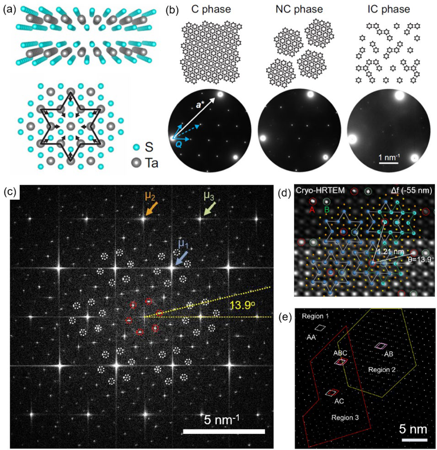
Atomic resolution high-angle annular dark-field- (HAADF) STEM imaging, coupled with FFT analysis, provides another approach to investigate the characteristics of PLD at the nanoscale (tens of nanometers). Lena et al. employed this technique to acquire real-space STEM images of the same region within a 1T-TaS2 thin film at both room temperature (293 K) and low temperature (∼ 95 K) using a Gatan 636 liquid nitrogen side-entry cold sample holder.[116] FFT analysis of these images revealed alterations in the reciprocal space features associated with the NC-to-C phase transition. Notably, the second-order satellite reflections adopted triangular patterns in both phases. However, compared to the C phase, the NC phase triangles exhibited a slight rotation and contraction, consistent with the previously reported diffraction-based structural changes in PLD. In addition, the first-order satellite peaks exhibited distinct characteristics. Specifically, the NC phase displayed three clusters of low-frequency satellite spots converging to a single point in the low-temperature C phase. Furthermore, the spatial variations observed in the shapes of the low-frequency satellite peaks across the TaS2 thin film suggested regional heterogeneity within the PLD structure. However, limitations inherent to FFT analysis hinder tracking structural changes at the atomic level (e.g., local defects, stacking faults). Direct examination of high-resolution TEM and STEM images remains essential for such investigations.
Directly resolving the atomic structural features of 1T-TaS2 PLDs in real space presents significant challenges. First, 1T-TaS2 thin film crystals exhibit high air and electron beam sensitivity, limiting the achievable dose for high-resolution atomic imaging using conventional TEM. Additionally, the CDW in 1T-TaS2 at low temperatures induces minimal atomic displacements. While low-temperature image drift correction algorithms can partially compensate for thermal drift from the cryogenic stage, they are insufficient to resolve the subtle, picometer-scale distortions of Ta atoms definitively. To overcome challenges associated with maintaining sample integrity during imaging, we developed a custom glovebox and vacuum interconnection system for transferring few-layer 1T-TaS2 flakes to a Cryo-TEM in an inert environment.[117,118] This approach preserves the material’s native structure. HRTEM was then performed using a Cryo-TEM with a DDEC camera that minimizes electron beam damage.[119] The Cryo-TEM’s integrated cold stage design minimizes vibrations, further enhancing image stability. Crucially, the DDEC camera’s electron counting mode reduces damage to the material’s intrinsic CDW structure. This is essential because our studies showed that conventional cameras disrupt the CDW phase at electron doses exceeding 3000 e−⋅Å−2, transitioning 1T-TaS2 from C-CDW state to NC-CDW state. DDEC cameras, on the other hand, excel at capturing the CDW structure at low doses, minimizing damage. Consequently, we successfully obtained atomic-resolution HRTEM images of mechanically exfoliated few-layer 1T-TaS2 well below the damage threshold. A representative FFT image (Fig. 5(c)) exhibits several satellite spots surrounding the Bragg reflection spots (indicated by arrows) originating from the underlying 1T-TaS2 lattice. These satellite reflections include first-order contributions due to the periodic lattice distortion (PLD), their corresponding second-order harmonics, and additional higher-order harmonics. The first-order satellite spots, highlighted by red circles and encircling the central transmission spot, correspond to three sets of PLD wave vectors with an identical wavelength (λ ≈ 1.21 nm). This indicates the formation of a
To directly analyze the real-space distribution of the periodic CDW superstructure in 1T-TaS2, HRTEM was employed with a defocus value of −55 nm. This defocus condition was chosen after careful analysis of the 1T-TaS2 contrast transfer function to optimize the visibility of the 1T-TaS2 atomic structure and the CDW superstructure. Subsequently, an inverse Fourier transform was applied to retrieve the real-space distribution of the superstructure based on first- and second-order satellite reflections. The resulting superstructure image was then overlaid onto the underlying atomic lattice image (Fig. 5(d)). This approach facilitated the direct visualization of the periodic distribution of the prominent satellite pattern, guided by the central bright spot of the superstructure. Our analysis revealed the presence of intrinsic interlayer misfit stacking in 1T-TaS2. Notably, the HRTEM data (Fig. 5(e)) unveils an interlaced domain structure within a ∼ 30 nm × 30 nm region, consisting of coexisting AA, AB, and AC stacking arrangements of SOD superstructures. Our results indicate that the dominant interlayer stacking for SODs in 1T-TaS2 adopts the TA configuration (where the centers of upper and lower SODs are well-aligned). However, the presence of localized TB or TC stacking interfaces (where the centers of the upper SODs are located on one of the six Ta atoms in the inner circle for TB configuration, or in the outermost peripheral of the lower SODs for TC configuration) within specific layers ultimately leads to the observed stacking domain structure (Fig. 5(e)). This observation is consistent with existing scanning tunneling microscope (STM) results, where most studies report a Mott insulating state in 1T-TaS2, which aligns with AA stacking. Conversely, a minority of studies have documented a reduction (AC stacking) or complete absence (AB stacking) of the Mott insulating gap at CDW domain walls.[110] These discrepancies can be attributed to the inherent complexity of the CDW stacking structure, as revealed by our HRTEM analysis. Our work represents a significant advancement in the understanding of 1T-TaS2 by providing the first direct observation of the intricate nature of the CDW stacking structure at the atomic level. These findings offer a microscopic explanation for the observed diversity of surface electronic states in this material. However, the HRTEM image merely presents the projection of SOD clusters in the z-direction, limiting the precise identification of the specific layer of the S–Ta–S molecular layer where the superstructure dislocation manifests. A comprehensive understanding of the stacking configuration of SOD clusters necessitates innovative technologies or methods. For example, the rapidly evolving 4D STEM technology can enhance in-plane resolution, offer nanoscale vertical structural insight, and support low-dose modes. In the future, it could be leveraged to unveil the complete 3D CDW stacking arrangement within 1T-TaS2.
Compared to dedicated Cryo-TEM with a fixed cryo-box in the pole pieces, side-insertion cryo-TEM presents a significant challenge for high-resolution atomic-scale structural analysis of quantum materials due to thermal drift. Lena et al.[120] implemented a combination of optimized STEM imaging methods and image post-processing algorithms to address this limitation. Notably, they employed a fast image acquisition strategy (< one second/frame) to track the sample drift during low-temperature STEM imaging effectively. However, this rapid acquisition approach comes at the expense of a compromised SNR in the acquired images, rendering established image alignment methods ineffective. They developed a dedicated rigid alignment algorithm to overcome limitations associated with image alignment in low SNR STEM images. This algorithm assumes only translational shifts within the image sequence and calculates relative offset matrices by cross-correlation between each image and all others. This approach facilitates more accurate identification and correction of image shifts, as demonstrated in Fig. 6(a). Notably, the algorithm is well-suited for crystalline samples, effectively mitigating artifacts and information loss arising from lattice distortions. Consequently, it enables precise investigations of picometer-scale features in quantum materials. Implementing this method enhances the resolution and SNR of low-temperature STEM images, facilitating the visualization of subtle lattice variations within charge-ordered phases.
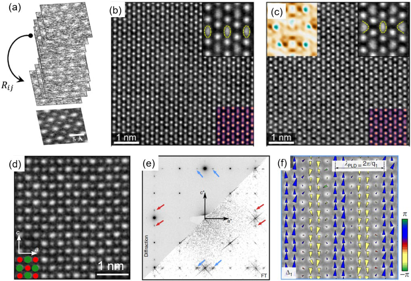
The same group employed a cryogenic sample rod within an aberration-corrected FEI Titan Themis TEM to acquire a series of HAADF-STEM images with short exposure times from 1T′-TaTe2 crystals maintained at 95 K. The acquired images were subsequently aligned and analyzed using their developed image post-processing algorithms. FFT analysis of the HAADF-STEM images revealed an image information transfer limit of 0.64 Å, enabling quantitative analysis of atomic positions.[121] These results demonstrate a unique PLD structure in 1T′-TaTe2 at low temperatures, which is in stark contrast to its structure at room temperature (Fig. 6(b)). Notably, every third Ta column remains structurally undistorted, while the intervening Ta columns exhibit a crescent-shaped distortion with a bending direction towards the undistorted columns (Fig. 6(c)). The observed PLD structure can be attributed to the movement of Ta atoms toward the structurally unperturbed columns, which successfully elucidated the low-temperature PLD microstructure of 1T′-TaTe2. Notably, manganate systems and other related oxides exhibiting charge order and PLD exhibit a distinct characteristic compared to 1T′-TaTe2. These materials possess coherent displacements strictly perpendicular to the electron beam direction, facilitating direct real-space displacement analysis through optimized Cryo-STEM imaging methods.
Building upon their recent development of the low-temperature STEM imaging method, Lena et al. combined it with a room-temperature STEM image-fitting technique for atomic polarization. This approach enabled a quantitative investigation of the evolution of lattice ordering in Bi0.35Sr0.18Ca0.47MnO3 (BSCMO) across a temperature range encompassing room temperature and liquid nitrogen temperature.[122] BSCMO, a perovskite manganite, exhibits a Curie transition temperature (Tc) near room temperature, with the ability to manipulate Tc through variations in dopant concentration. To elucidate the structural changes associated with charge ordering in BSCMO, the authors acquired HAADF images at room temperature (near Tc) and liquid nitrogen temperature (far below Tc). Undistorted reference images were generated by selecting specific Bragg reflections and performing inverse Fourier transforms. Subsequently, quantitative picosecond-level maps of PLDs were obtained by fitting the atomic positions within the original and reference images. Quantitative determination of the PLDs in BSCMO at room temperature was first achieved using STEM imaging, revealing domains of approximately 5 nm and suggesting a complex mesoscopic charge order within the material. Direct observation confirmed lateral atomic displacements on both the A-site (Bi/Sr/Ca) and B-site (Mn) relative to the modulation vector. These displacements were quantified as 6 pm–8 pm, consistent with a “stripe” charge order characterized by paired antiparallel stripes and unit cell tripling. Notably, the modulated wave vector at room temperature exhibited incommensurability with the underlying Bragg lattice (q ≈ 1/(3a*)). However, upon cooling to liquid nitrogen temperature, a transition from an incommensurate to a commensurate phase (q = 1/(3a*)) was observed in the charge order.
Figure 6(d) presents a low-temperature HAADF-STEM image of BSCMO. The corresponding montage of FFT patterns and the electron diffraction image are shown in Fig. 6(e), where red and blue arrows highlight the satellite spots indicative of the PLD superstructure. Figure 6(f) displays the extracted PLD mapping, revealing a stripe-like charge order with a supercell three times larger than the Bragg unit cell, consistent with observations at room temperature. Triangles in Fig. 6(f) represent the displacements of the corresponding atomic columns, with their area proportional to the displacement amplitude. Notably, the PLD modulation in BSCMO is predominantly along the c-axis (indicated by opposite directions for blue and yellow triangles), with a weaker modulation observed along the a-axis. Compared to the room-temperature PLD mapping, the low-temperature charge order distribution exhibits enhanced uniformity and periodicity. Notably, electron diffraction (μm field of view) revealed a significant difference in the average wavevector (q) values at 293 K (0.314 rlu) and 95 K (0.332 rlu). Conversely, local high-resolution STEM measurements (17 nm–40 nm field of view) displayed q variations, likely attributable to local phase inhomogeneity. These discrepancies underscore the inherent heterogeneity of the charge order and the complexity of charge order domains, highlighting the necessity of high-resolution techniques for resolving such features.
-
Beyond investigating charge order in quantum materials, Cryo-TEM has emerged as a valuable tool for exploring topologically non-trivial spin textures. This application necessitates significantly lower temperatures, as the phenomena of interest frequently manifest in the liquid helium temperature regime, unlike those observable with liquid nitrogen.[104] Furthermore, many intriguing spin configurations exhibit stability only within a very restricted window of their temperature-phase diagram.[105] The non-trivial topological nature of magnetic configurations manifests as a topological Hall effect arising from the Berry phase.[123] In such materials, the spin of transmitted electrons aligns with the spatially varying magnetization. Consequently, TEM-based investigations of spin textures in quantum materials predominantly rely on implementing Lorentz phase transmission electron microscopy (LTEM) in conjunction with liquid helium sample stages. LTEM offers the capability for in-situ, non-destructive observation of real-space spin structure changes within a sample under the application of a magnetic field. Although the spatial resolution of LTEM is lower than that achievable with conventional TEM/STEM, and liquid helium stages exhibit more significant thermal drift compared to their liquid nitrogen counterparts, the attainable 10 nm resolution remains sufficient for resolving individual spin textures in most materials and tracking their crystallization/melting processes under variations in temperature and magnetic field.[105]
The Zhu group demonstrated the controllable manipulation of skyrmions in Te-doped multiferroic Cu2OSeO3 (CSO) thin films using liquid-helium-temperature LTEM.[124] They systematically investigated the evolution of the helical and skyrmion phases as a function of temperature (12 K–20 K), magnetic field, Te doping level, and sample thickness. At low temperatures, the CSO films exhibited a magnetic phase transition from the helical phase to the skyrmion phase with an increasing applied magnetic field. The initial observation reveals an anisotropic scaling behavior of the helical phase periodicity. Upon application of a magnetic field, the modulation period of the h[110] phase exhibits a significant expansion accompanied by a clockwise rotation, reaching a maximum angle of approximately 15° (Fig. 7(a)). Conversely, the modulation period of the h[001] phase shows minimal change, although its projected area progressively decreases with increasing magnetic field strength. Notably, the study revealed a “channel phenomenon” for skyrmion propagation. Skyrmion chains nucleate at the edge of the helical phase within the thin sample region and propagate through the helical phase towards the thicker sections under an increasing magnetic field (Fig. 7(b)). This preferential propagation occurs along the h[001] spiral direction, leading to the sequential filling of different thickness regions with the skyrmion spin texture. Interestingly, two distinct nucleation sites for skyrmions were observed within the thin section, forming two populations (SkL1 and SkL2) characterized by wave vectors with a 30° inclination relative to each other. As the magnetic field intensity increased, SkL1 became the dominant population, eventually encompassing the entire sample. Further intensification of the magnetic field triggered localized instabilities within SkL1, manifesting as rotations and the emergence of moiré patterns in confined regions. This suggests a loss of coherence in wave vectors between neighboring sections. Subsequently, SkL1 expanded and exhibited a clockwise rotation up to 30° , ultimately transitioning into a uniform ferromagnetic phase. Theoretical investigations posit that the out-of-plane tilt of the helix is responsible for the helical periodicity’s observed anisotropic and non-linear scaling behavior.
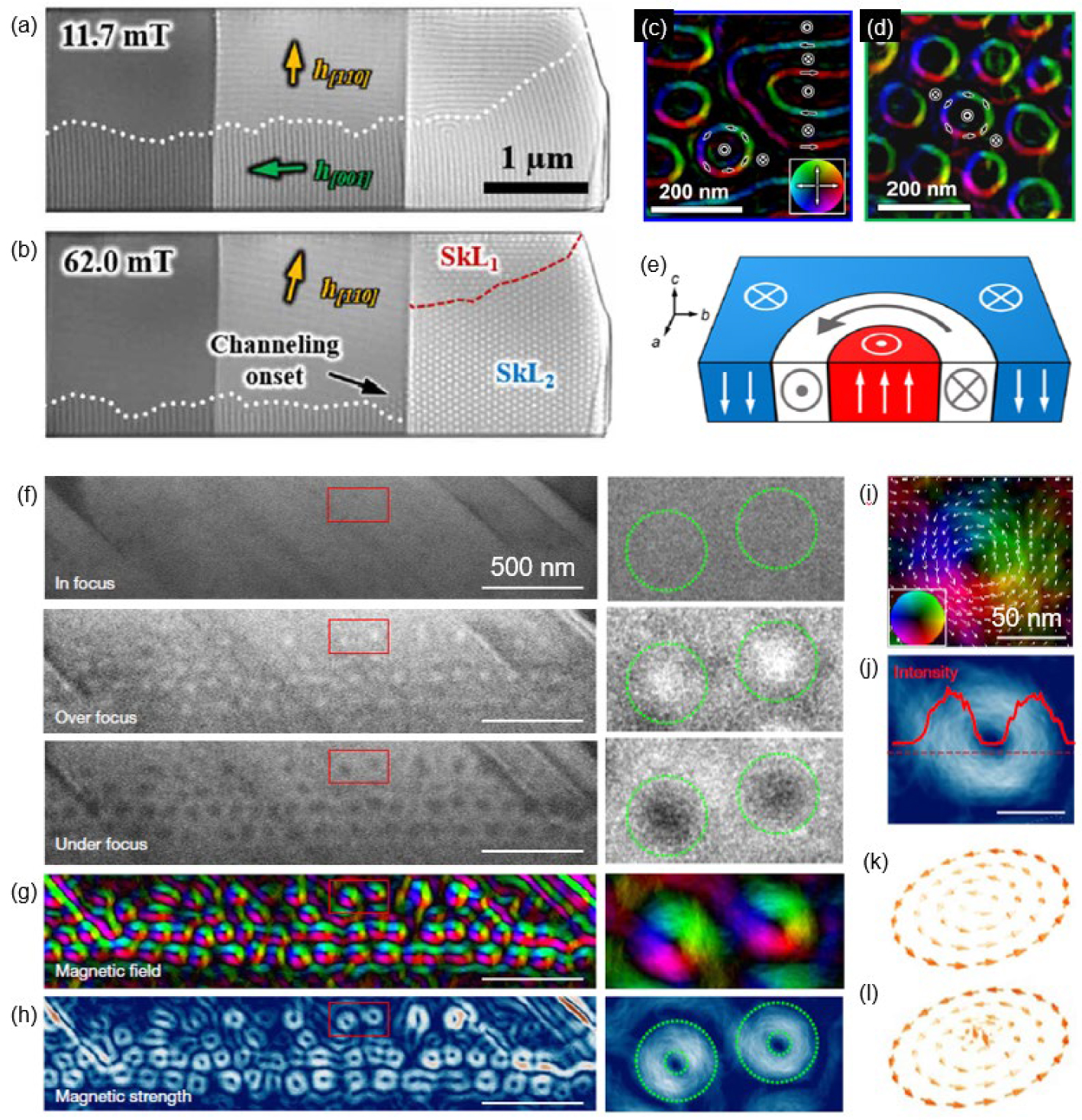
Zhu et al. further exemplified spin texture observation using liquid-helium-temperature LTEM to investigate topological spin states and skyrmion bubbles in the 2D insulating van der Waals material Cr2Ge2Te6.[125] This ferromagnetic insulator possesses a band gap of ∼ 0.74 eV and exhibits uniaxial solid magnetic anisotropy with an easy axis of magnetization perpendicular to the ab plane. These attributes render Cr2Ge2Te6 a model system for studying skyrmion bubbles. Their findings demonstrate that the material’s robust intrinsic perpendicular magnetic anisotropy leads to the spontaneous formation of stripe domains in exfoliated thin films (Fig. 7(c)). Upon cooling under an external field applied perpendicular to the plane, competition between dipolar interactions and uniaxial magnetic anisotropy leads to the formation of a hexagonally packed nanobubble lattice (Fig. 7(d)). During the dynamic transition from stripe domains to bubbles, the nucleation and annihilation of Bloch line pairs within the stripes induce spin rotations confined to the Bloch walls. Individual Bloch lines act as topological defects harboring a ±1/2 magnetic charge. Notably, the total integer topological charge associated with each stripe or bubble is conserved throughout pair formation and annihilation. This conservation facilitates a topological transition between type I and type II stripes (the authors defined the narrow strip domains bounded by two antiparallel Bloch walls as type I stripe and the other stipe domains with two parallel Bloch walls as type II), showcasing the diverse spin textures realizable in 2D ferromagnets (Fig. 7(e)). Furthermore, it presents a novel platform for engineering exotic quantum states through magnetic proximity effects.
Wang et al. pioneered the direct observation of topological spin texture within the pseudogap phase of YBa2Cu3O6.5 (YBCO) using a low-drift liquid-helium platform and low-temperature LTEM.[126] Rectangular, wedge-shaped YBCO TEM samples were fabricated via focused ion beam (FIB) milling. This preparation method, resulting in samples with a thickness gradient, proved advantageous for identifying the region exhibiting optimal LTEM signal contrast. Figure 7(f) presents LTEM images acquired under zero-field conditions (300 K, Δf = ± 1.08 mm) utilizing the in-focus, over-focus, and under-focus Fresnel modes of LTEM. Quantitative phase analysis (QPA) was performed on these images using QPt software based on the transport of intensity equation (TIE) method. This analysis enabled the extraction of the real-space spin texture (Fig. 7(g)) and the corresponding field strength (Fig. 7(h)). Enlarged insets are provided for each image in the right panels of Figs. 7(f)–7(h). Figure 7(i) employs a color wheel to represent the in-plane component of the magnetic field vector for each spin texture. In this scheme, chromaticity and color saturation encode the field direction and magnitude, respectively (Fig. 7(j)). Liquid-helium-temperature LTEM directly retrieves a sample’s in-plane magnetic field component by analyzing the high-resolution spatial deflection of the incident electron beam. This principle inherently restricts its sensitivity to the magnetic field component perpendicular to the electron beam direction (i.e., the a–b crystal plane). Consequently, the observed spin texture in the YBCO cross-sectional sample aligns with those depicted in the schematic diagrams of Figs. 7(k) and 7(l). These findings provide real-space microscopic evidence suggesting time-reversal symmetry breaking below the characteristic temperature (Tc). This study further refines the phase diagram region for the existence of the YBCO topological spin texture and highlights the critical role of orthogonal-II type oxygen ordering and appropriate sample thickness for its observation using this technique.
3.1. Charge ordering
3.2. Spin textures
-
This review offers a comprehensive analysis of recent advancements in Cryo-TEM. We begin by dissecting the interaction mechanism between imaging electrons and atomic structures, establishing a foundation for systematically examining the principles governing electron beam-induced structural damage in sensitive materials. Subsequently, we explore the advantages of Cryo-TEM and its associated hardware and software for imaging electron-beam-sensitive materials. We then delve into dose-efficient Cryo-TEM imaging methods, showcasing their applications and contributions to the structural elucidation of crystalline materials containing organic components. Furthermore, we examine the latest progress in utilizing Cryo-TEM technology to unveil novel quantum phenomena in emerging quantum materials, with a particular focus on charge order and spin texture properties. The burgeoning prominence of Cryo-TEM in materials and physical sciences has spurred rapid development in related technologies and methodologies. This advancement has opened new avenues for accelerating the discovery of novel materials and facilitating the practical implementation of quantum information science. As we look ahead, the future development of Cryo-TEM presents both challenges and exciting opportunities for further exploration.
A prominent challenge in Cryo-TEM is achieving precise and continuous control over a more comprehensive temperature range, particularly for lower temperatures. Biological Cryo-TEM typically operates stably only at liquid nitrogen temperature (∼ 77 K). While side-insertion holders offer variable-temperature capabilities (liquid nitrogen or liquid helium to room temperature), these methods often suffer from thermal drift under dynamic conditions, hindering atomic-resolution imaging. Future advancements should prioritize the development of mechanically robust systems capable of maintaining ultra-low temperatures (below 1 K) and enabling continuous temperature control. Such harsh requirements may necessitate novel instruments integrating superconducting cooling systems and electron optical devices with exceptional stability and high spatial and energy resolution. Such advancements would unlock a broader range of temperature-dependent experiments, including investigations of the structural properties and electronic behavior of superconducting materials below their Tc and studies of lattice dynamics in quantum phase transition materials near their critical points.
Another promising direction for Cryo-TEM advancement lies in integrating diverse in-situ techniques within the imaging system. These techniques could encompass in-situ application of electric fields, optical manipulation, mechanical stimulation, and gas-phase environments. Cryo-TEM and in-situ TEM have emerged as transformative advancements significantly impacting materials research. Their synergistic integration holds immense potential to deliver the next generation of transformative materials and physical sciences research tools. One potential approach for integrating in-situ techniques with cryogenic environments involves the development of microelectromechanical systems (MEMS) chip technology. MEMS chips could be used for electrical measurements or to investigate bias-induced phenomena through micro-lines under ultra-low temperatures. Another promising avenue lies in the development of ultrafast optical components. This approach would enable the utilization of pulsed electrons to capture ultrafast phenomena and transient material structures in-situ during quantum phase transitions.
Beyond low-temperature, for in-situ studies, current instrumentation for structural characterization of electron-beam-sensitive materials encounters limitations in low-dose detection capabilities. While these techniques can visualize functional groups in organic crystals, the achievable magnification at tolerable doses falls short of atomic resolution, hindering the clear visualization of light elements (C, N, O). This limitation is particularly critical for materials like all-organic perovskite crystals, where the structural integrity threshold dose is lower than the quantum limit for light atom structure determination in TEM.[127] To overcome these limitations and achieve true atomic resolution or quantify structural distortions of light atoms, future advancements necessitate innovations on two fronts. First, breakthroughs are needed to enhance the dose tolerance of organic crystals. Second, improvements in the quantum detection efficiency of cameras are crucial. This could involve developing novel imaging algorithms that utilize electron scattering patterns for precise atomic localization and structure reconstruction from minimal data. Beyond achieving superior spatial resolution for the atomic structure of sensitive materials, future Cryo-TEM development should also prioritize advancements in energy resolution and overall efficiency. Such advancements would unlock near-atomic resolution detection of sensitive materials’ intrinsic electronic state structure, such as organic molecules, using energy-filtered EELS in Cryo-TEM.
 DownLoad: