
 首页
首页 登录
登录 注册
注册


HTML
-
Transparent conductors (TCO) represent a class of functional materials characterized by high electrical conductivity and high transmittance within their characteristic spectral ranges.[1] Over the last few decades, visible transparent conductors have been widely applied in multiple optoelectronic devices, such as flat-panel displays,[2,3] solar cells,[4,5] and touch-panel screens.[6,7] Recent technological advances in infrared detectors,[8] infrared photovoltaic devices,[9] and electromagnetic shielding[10,11] have driven an increased demand for transparent conductors operating in the infrared spectral band (commonly 2.5–25 μm).
The exploration of high-performance infrared transparent conductors has extended across multiple material systems, notably conductive oxides,[12] low-dimensional carbon materials,[13,14] and chalcogenides.[15] However, to the best of our knowledge, an inherent conflict between high infrared transmission and outstanding electrical conductivity is universally observed in all aforementioned systems. Oxide conductors are typically subject to a blue shift in the infrared transparency band while enhancing conductivity through methods like doping.[12,16] Chalcogenide films, such as Bi2Se3,[15] CdSe,[9] and LaSe2,[17] exhibit superior electrical conductivity with sheet resistance below ∼ 100 Ω/sq, yet their optical transmission performance is significantly diminished at wavelengths beyond 10 μm (far-infrared region). In contrast, while manifesting broadband infrared transparency, low-dimensional carbon materials require further enhancement in electrical conductivity (sheet resistance ∼ 500 Ω/sq).[18,19] Therefore, an urgent unmet need persists for functional materials that simultaneously achieve high optical transmittance and electrical conductivity across the broad infrared band (2.5–25 μm).
Indium tin oxide (ITO) films are currently the most commonly used transparent conductors[20,21] in commercial applications, owing to their excellent visible transparency, high electrical conductivity, low thermal resistance,[2] and large-area uniformity.[22] Previous studies have shown that conventional ITO films possess reflectance exceeding 0.80 in the Infrared region with wavelengths above ∼ 2 μm,[23–25] which severely limits the application potential as infrared transparent conductors. Consequently, optimizing the infrared transmittance of ITO films constitutes an essential prerequisite for improving the infrared optoelectronic performance. Reducing the film thickness has been demonstrated to provide a simple yet effective method to achieve this optimization.[26,27] For metallic thin films, when the thickness is below the optical penetration depth determined by the skin effect, reduced surface reflectance and enhanced infrared transmittance are observed as the optical field can fully penetrate through the film.[28,29] Additionally, the multiple reflections of incident light between the top and bottom surfaces of the thin film also have the potential to increase transmittance through interference enhancement.[26] However, reducing the thickness of ITO films leads to a significant increase in the sheet resistance. Particularly, for ITO films with thicknesses below a few tens of nanometers, reduced relaxation time,[30] carrier localization,[31] and the insulating dead-layer induced by interfacial defects[30] further degrade their conductive performance. Therefore, it is imperative to take additional measures to maintain the electrical conductivity while reducing the thickness of ITO films for enhanced infrared transmittance.
Experimental studies have discovered that introducing oxygen vacancies and constructing stacked architectures with ultra-thin metal films represent two effective strategies for significantly improving the electrical conductivity of ITO films. The oxygen vacancies in ITO films act as doubly ionized donors,[32] with each vacancy donating two free electrons. Consequently, under the assumption of unchanged carrier mobility, the introduction of oxygen vacancies enhances electrical conductivity by increasing the carrier concentration. Nevertheless, excessive oxygen vacancies can enhance the infrared reflectance[33] by shifting the near-infrared reflectance edge to shorter wavelengths,[34] which critically compromises the infrared transmittance. Therefore, establishing an oxygen vacancy concentration threshold to optimize the trade-off between the electrical conductivity and the infrared transparency emerges as a crucial engineering objective.
For metal/ITO stacked films, the ultra-thin metal layer typically exists in the form of an interlayer[35,36] sandwiched between ITO layers or as a capping layer.[37,38] Owing to their low resistivity (∼ 10−6 Ω·cm), metals such as Au, Ag, Cu, and Al are typically selected as the ultra-thin metal layer materials.[39] The overall conductance of the metal/ITO stacked films is significantly enhanced due to the parallel conductive network formed between the ultra-thin metal layer and the ITO layer. However, maintaining the infrared transmittance of metal/ITO stacked films requires precise control of the thickness of the metal capping layer. Numerous studies suggest that the metal/ITO systems exhibit a strong positive correlation between the infrared reflectance in wavelengths above ∼ 2 μm and the metal layer thickness.[40,41] To achieve high infrared transmittance, the thickness of the metal capping layer must be reduced below ∼ 5 nm.[42,43] However, decreasing the thickness of ultra-thin metal films facilitates the formation of discrete metallic islands and semi-continuous morphologies,[44] leading to a dramatic rise in electrical resistivity[45,46] or even triggering a metal–insulator transition.[47] Therefore, determining the optimal thickness threshold for ultra-thin metal layers constitutes a critical challenge in optimizing the infrared optoelectronic performance.
According to the aforementioned analysis, the independent modulation strategies of oxygen vacancy content and the ultra-thin metal capping layer for enhancing the electrical conductivity of ITO films may both be constrained by the requirement to maintain the infrared transmittance. Based on the parallel conductive network formed between the ultra-thin metal capping layer and the ITO film, the combined effect of these two modulation mechanisms is anticipated to further optimize electrical conductivity while maintaining infrared transmittance.
Thus, the present study has constructed a metal/ITO bilayered film system by using DC magnetron sputtering technology, aiming to optimize the optoelectronic properties in the 2.5–25 μm infrared spectral range through the combined effect of oxygen vacancy content and ultra-thin metal layers. The ITO film thickness is tailored to ∼ 20 nm to enhance the infrared transmittance, while Cu is selected as the ultra-thin metal capping layer material based on its high conductivity, low cost, and environmental stability. Prior to constructing Cu/ITO bilayered films, systematic investigations are conducted to unravel the correlation between oxygen vacancy concentration and the infrared transmittance–sheet resistance relationship in pristine ITO films. Preliminary studies also demonstrate that the optoelectronic enhancement of ITO films by ultrathin copper overlayers exhibits critical thickness dependence. Based on these findings, investigations on Cu/ITO systems reveal that the combined effect of moderate oxygen vacancy content and ∼ 3 nm Cu capping layer not only optimizes charge carrier pathways but also maintains high infrared transmittance by suppressing surface/interface scattering and absorption, enabling the Cu/ITO films to achieve an average infrared transmittance of ∼ 0.861 and a sheet resistance of ∼ 400 Ω/sq. This discovery highlights the critical importance of the combined effect of metal/ITO heterostructure construction and oxygen vacancy content control strategies in optimizing the infrared-transparent conductive properties.
-
Pristine ITO and Cu/ITO films are deposited on silicon wafers, silica optical glass substrates, and KBr wafers by direct current (DC) magnetron sputtering at room temperature. Prior to being introduced into the vacuum chamber, these substrates are cleaned in anhydrous ethanol and deionized water in an ultrasonic bath for 10 minutes each. Following this, the vacuum chamber is evacuated to a base pressure of 1.0 ×10⁻³ Pa. For pristine ITO films, an In2O3 (90 wt%) : SnO2 (10 wt%) target with a diameter of 100 mm is pre-sputtered in a pure argon atmosphere for 5 min to remove the surface contamination. The film deposition process is carried out in an argon-oxygen atmosphere at a total pressure of 0.25 Pa and a fixed O2/Ar pressure ratio of 2.5%. The sputtering power is set to 40 W, 60 W, 80 W, and 120 W, respectively, while other experimental conditions remain unchanged. The thicknesses of ITO layers or pristine ITO films are fixed at approximately 20 nm. The obtained ITO films are designated as 40 W-ITO, 60 W-ITO, 80 W-ITO, and 120 W-ITO, respectively.
For ultra-thin Cu layers, a similar pre-sputtering process is also carried out to remove the possible oxide layer formed on the target surface. The copper layers are deposited at a sputtering power of 40 W, while the deposition atmosphere is high-purity argon with a fixed gas pressure of 0.50 Pa.
In order to analyze the compositional variations in ITO films, x-ray photoelectron spectroscopy (XPS) measurements are performed using a PHI 5000 VersaProbe spectrometer. The binding energy scale has been calibrated by assigning the C 1s peak originating from adventitious carbon contamination at 284.8 eV. In standard stoichiometric In2O3–SnO2 films, it is expected that each indium (In) and tin (Sn) atom is bonded to an average of 1.5 and 2.0 oxygen (O) atoms, respectively. Therefore, we employ the parameter α to evaluate the overall oxygen content in as-deposited ITO films:[48]
where I(O), I(In), and I(Sn) correspond to the sensitivity-factor-normalized peak areas of O 1s, In 3d5/2, and Sn 3d5/2, respectively. For the ideal stoichiometric In2O3–SnO2 films, the value of α is 1.
Moreover, x-ray reflectivity (XRR) measurements are carried out on Cu/silicon samples using a Rigaku-Smartlab x-ray diffractometer equipped with a Cu Kα radiation source (λ = 0.15406 nm). The XRR intensities have been recorded over an angular range from 2θ = 0° until all periodic oscillations originating from Kiessig fringes[49] are damped out by the film roughness,[50] typically before 2 θ = 6°. For ultra-thin Cu films, the XRR data are fitted using the Genetic algorithm method, regarding film thickness, film density, and surface roughness as fitting variables. The surface morphology of Cu/ITO films has been investigated by using an atomic force microscope (AFM, MFP-3D Origin, Oxford Instruments). Surface roughness height maps are acquired during the lateral motion of the tip at a fixed scan rate of 2 Hz.
The films used for infrared transmittance measurements are deposited on KBr substrates which exhibit an infrared transmittance exceeding 0.85 across the entire infrared (IR) region (2.5–25 μm). Fourier transform infrared spectroscopy (FTIR) spectra of ITO, Cu, and Cu/ITO films are recorded by using a Bruker FTIR analyzer in transmittance mode at room temperature. The transmittance spectra of pristine KBr wafers is recorded as a background signal before the sample is measured. Thus, the contribution from the KBr substrate has been subtracted from the transmittance spectra of the film. The KBr wafers are placed in a holder that is perpendicular to the direction of infrared waves. To systematically quantify the infrared transmittance characteristics, an average transmittance parameter, Tave, is defined as follows:
The values of parameters λmin and λmax are set to 2.5 μm and 25 μm, respectively.
The sheet resistance of pristine ITO and Cu/ITO films deposited on silica optical glass substrates has been determined by means of a standard four-point probe platform (HPS 2524). The four collinear, equally spaced probes function with the outer pair passing current through the sample, while the inner pair measures the resulting potential difference.[51] The high input impedance (> 1 GΩ[52,53]) of the voltmeter in the test platform ensures that the current through the voltmeter is negligible compared to the sample current, making parasitic voltage drops from contact resistance insignificant.[52] As the current through the sample equals the source current output, the effects of contact resistance on film conductivity are eliminated in four-point probe measurements. During the test, the sample has been fixed on the platform and the four probes are lowered to closely contact the surface of the samples.[54] For the sake of minimizing measurement error, the overall sheet resistance is determined by averaging the measurement results from six different positions for each sample.
For a comprehensive evaluation of the optoelectronic performance of ITO films, the figure of merit (FOM) is calculated by using the Haacke equation[55] as follows:
where Tave is the average infrared transmittance and RS denotes the sheet resistance.
-
In order to investigate the effect of sputtering power on the oxygen content, XPS measurements have been carried out on pristine ITO films. It is found that the In 3d XPS spectra exhibit a characteristic spin–orbit doublet with binding energies of 444.4 eV (In 3d5/2) and 451.9 eV (In 3d3/2), demonstrating the exclusive presence of the In3+ oxidation state (not shown).[48] Furthermore, detailed Sn 3d5/2 and O 1s spectra are presented in Figs. 1(a) and 1(b), respectively. As shown in Fig. 1(a), the Sn 3d5/2 signal is deconvoluted into two symmetric components by assuming the coexistence of two distinct chemical states of tin. The main peak at ∼ 486.20 eV is ascribed to the presence of Sn2+, while the weak shoulder peak corresponding to Sn4+ is observed to shift towards the higher binding energy side by ∼ 0.70 eV with respect to the Sn2+ 3d5/2 component.[56,57] In Fig. 1(b), it is observed that the O 1s XPS spectra are resolved into three Gaussian components.[58,59] The first O 1s peak located at ∼ 529.50 eV is attributed to the typical In–O bonds in the lattice structure (marked as Olat hereafter). The second Gaussian component peaks at ∼ 531.40 eV and corresponds to the chemisorbed oxygen species at the film surface (denoted as Ochem). The last O 1s component, centered at approximately 533.0 eV, is related to the adventitious species weakly bound to the film surface, such as water molecules or organic contaminants (denoted as Oabs hereafter).
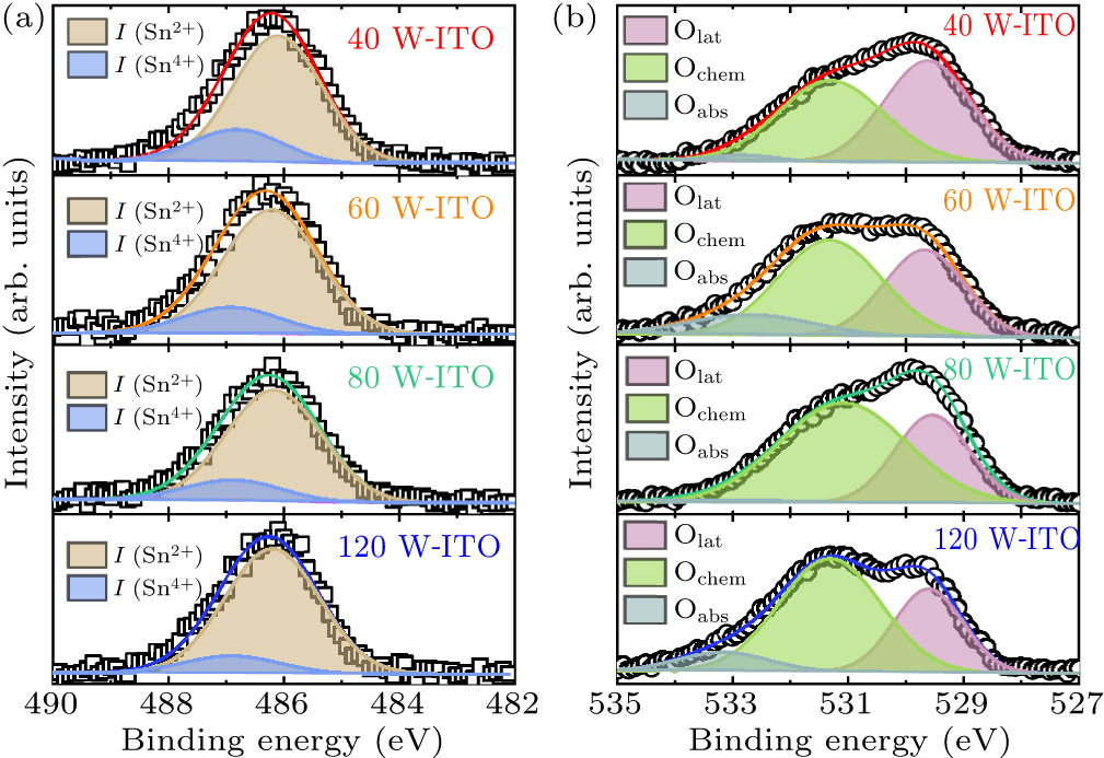
The variations of surface stoichiometry in ITO films are determined from the corresponding peak areas and corrected using sensitivity factors, as summarized in Fig. 2. As exhibited in Fig. 2(a), it is found that the Sn/In atomic ratio in ITO films remains nearly constant (ranging from 0.088 to 0.092) as the sputtering power increases from 40 W to 120 W, which is in good agreement with the nominal Sn/In stoichiometry (0.102) of the target. Detailed fitting results show that Sn2+ accounts for over 80% of the total tin content in all cases, which is attributable to the presence of oxygen vacancies. Moreover, ITO films deposited at higher sputtering powers exhibit a higher atomic ratio of Sn2+/Sn4+, as displayed in Fig. 2(b), suggesting that increased sputtering power promotes a rise in the oxygen vacancy concentration.
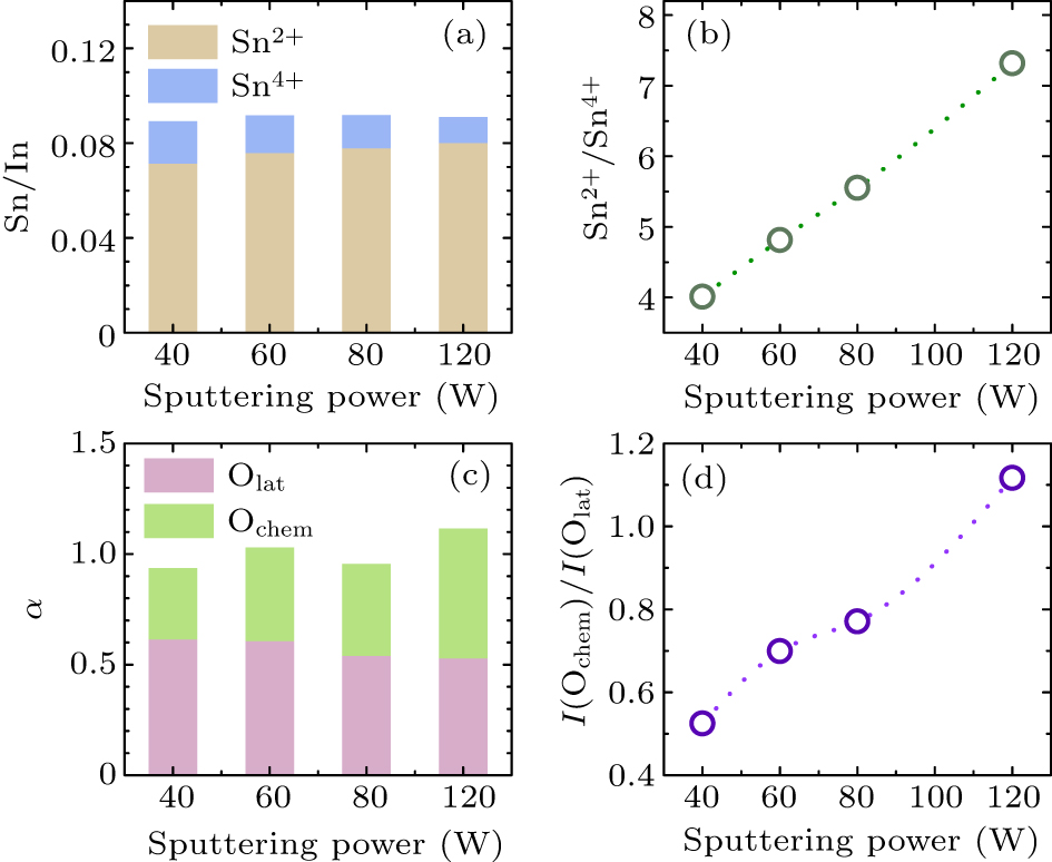
The relationship between sputtering power and oxygen vacancy content is further confirmed by quantitative analysis of the O 1s spectra. The respective contributions of Olat and Ochem to the total oxygen content were determined, while the Oabs component from surface contamination was excluded. Using Eq. (1), the total oxygen content was found to approach near-stoichiometric levels through the combined effects of lattice oxygen and chemisorbed oxygen species (Fig. 2(c)). Previous studies have shown that chemisorbed oxygen primarily arises from the inevitable dissociative adsorption of water molecules from air onto oxide film surfaces.[60,61] In this process, surface oxygen vacancies are oxidized by water molecules, forming hydroxyl groups which represent the primary manifestation of chemisorbed oxygen species. Accordingly, the oxygen vacancy concentration can be qualitatively estimated from the relative amount of chemisorbed species, as shown in Fig. 2(d). As evident from the data, oxygen vacancy concentration increases with sputtering power, in agreement with earlier reports.[62,63] This result suggests that by adjusting sputtering power, one can systematically investigate how oxygen vacancies affect the optoelectronic performance of pristine ITO films.
The infrared transmittance spectra of ITO films deposited under different sputtering powers are presented in Fig. 3(a). In general, all ITO thin films exhibit relatively high transparency in the infrared region, likely due to the suppression of absorption and reflection loss by the reduced film thickness. The 40 W-ITO film becomes almost completely transparent in the range of 2.5–14 μm as it exhibits a high transmittance of 0.990. At longer wavelengths, the transmittance of the 40 W-ITO film shows a slow decrease and achieves a minimum of 0.926 at 25 μm. The 60 W-ITO film exhibits transmittance spectra similar to those of the 40 W-ITO film, with a slight reduction in absolute transmittance values. Compared to 40 W-ITO and 60 W-ITO films, the 80 W-ITO film exhibits both a rapid wavelength-dependent decline in infrared transmittance (dropping from 0.945 at 2.5 μm to 0.835 at 25 μm) and consistently lower absolute values across the entire IR region. The 120 W-ITO film demonstrates the lowest infrared transmittance and the most pronounced transmittance attenuation as the wavelength increases, exhibiting a reduction from T = 0.950 at 2.5 μm to T = 0.697 at 25 μm. Thus, ITO samples prepared under higher sputtering powers show lower absolute transmittance values and more rapid transmittance attenuation. We also calculated the average transmittance Tave using Eq. (2), which reveals a monotonic decline in Tave with increasing sputtering power (shown in Fig. 3(b)). Based on the correlation between oxygen vacancy concentration and sputtering power, this trend demonstrates that an increase in oxygen vacancy content exerts a suppressive effect on infrared transmittance.
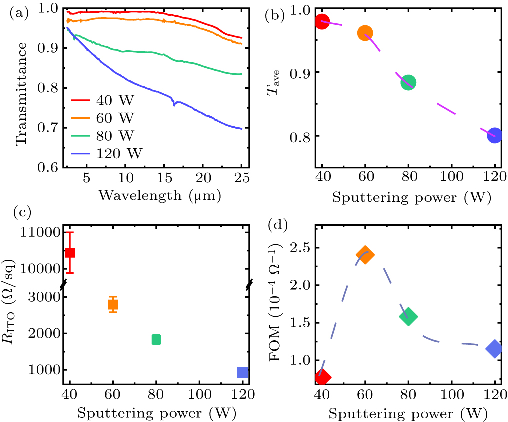
The sheet resistance of pristine ITO films (marked as RITO) as a function of the sputtering power is shown in Fig. 3(c). It is clearly observed that the 40 W-ITO film exhibits the highest sheet resistance of ∼ 10000 Ω/sq among all the ITO samples. With increasing sputtering power to 120 W, the sheet resistance of ITO films gradually decreases, reaching a minimum of ∼ 935 Ω/sq in the 120 W-ITO sample. Given that both x-ray diffraction (XRD) out-of-plane scans and scanning electron microscopy (SEM) characterizations confirm an amorphous structure across all sputtering power conditions (not shown), the observed gradual decrease in sheet resistance suggests that the increased oxygen vacancy content improves the conductivity of ITO films.
Since each oxygen vacancy donates an average of two free electrons to the lattice, the infrared transmittance and electrical conductivity of ITO films can be correlated through the dynamical modulation of carrier density. According to Drude theory, an increase in free carrier density within ITO films significantly enhances electrical conductivity[64] under constant electron effective mass and relaxation time. Nevertheless, this enhancement concurrently intensifies photon absorption[65,66] in the infrared spectrum, while the increased conductivity reduces the optical penetration depth of infrared waves. The combined effect of optical absorption and reflection loss ultimately results in the suppression of infrared transmittance. Based on the trade-off relationship between infrared transmittance and electrical conductivity in pristine ITO films, we employ FOM calculations to identify the best compromise between these two properties. FOM calculation results are presented in Fig. 3(d). As evidenced by the data, the 60 W-ITO film with high infrared transmittance yet compromised electrical conductivity (sheet resistance as high as 2400 Ω/sq) achieves the highest FOM value, however, as shown in 80 W-ITO and 120 W-ITO films, attempts to further enhance conductivity by increasing oxygen vacancy densities result in rapid infrared transmittance attenuation and subsequent FOM decline. To address this inherent trade-off, we strategically introduce an ultra-thin Cu capping layer that possesses substantial potential for enhancing electrical conductivity while minimizing transmittance loss, thereby improving the overall infrared optoelectronic performance.
-
As the copper layer thickness has been widely documented to significantly affect the optoelectronic performance of Cu/ITO stacked films,[37,67] we aim to find the optimized Cu capping layer thickness for the infrared optoelectronic properties of Cu/ITO bilayered films. Thus, on substrates of silicon wafers, KBr wafers, and silica optical glass substrates, an ITO layer with identical thickness and properties to the 40 W-ITO film is deposited first, followed by the deposition of an ultra-thin Cu capping layer. The deposition time of the Cu capping layer is set to 20 s, 24 s, 30 s, and 36 s to pursue continuous adjustment of its thickness. Additionally, ultra-thin Cu films with identical corresponding deposition times (20 s, 24 s, 30 s, and 36 s) are also directly deposited on silicon wafers (denoted as Cu/silicon), to determine the thicknesses of Cu layers without influence from the ITO bottom layer.
In order to gain more insight into the deposition mode and surface morphology of ultra-thin Cu layers, AFM measurements were performed over a 1.5 μm × 1.5 μm scanning area on the pristine 40 W-ITO film (without a Cu capping layer) and a Cu-20 s/40 W-ITO sample with a Cu capping layer deposited for 20 s, respectively. As shown in Fig. 4(a), the AFM scans reveal a rather smooth surface of the pristine 40 W-ITO film. Nevertheless, for the Cu-20 s/40 W-ITO sample (shown in Fig. 4(b)), well-separated islands or hillocks formed by Cu nanoparticles are observed on the surface of the bottom ITO layer. These Cu hillocks exhibit semi-ellipsoidal profiles, displaying a non-uniform distribution and relatively low surface coverage. Similar observations have been reported in studies of other ultra-thin metal films,[68,69] reflecting the prevalence of three-dimensional (3D) island-like growth modes in such systems.[70,71] During the initial stage of thin-film growth, the deposited atoms tend to aggregate at specific nucleation sites on the substrate surface[72] due to the strong interatomic attractions,[70] thereby promoting the formation of isolated metal clusters[73] and the emergence of 3D island structures. As the deposition process progresses, the diffusion of Cu atoms drives the lateral extension of isolated islands[70] and the formation of a continuous network, resulting in film growth proceeding in a typical layer-by-layer mode.[74] Consequently, the Cu ultra-thin layers may develop a mixed island-layer structure, particularly evident in samples subjected to longer Cu capping layer deposition time.
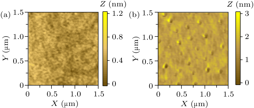
Figure 5(a) shows the XRR spectra of the as-deposited Cu/silicon films. Extensive parameter fitting reveals significant deviations between the experimental data and the theoretical XRR curve for an ideal single layer. Nevertheless, the XRR spectra above the critical angle are effectively fitted using a two-layer model consisting of a low-density intermediate layer and a bulk-like layer. The detailed fitting parameters are summarized in Table 1. This finding aligns with the hypothesis that the ultra-thin Cu layer exhibits a mixed island-layer structure, evidenced by the low-density intermediate layer, which suggests island formation with voids, contrasting with the denser bulk-like layer, which indicates a layer-by-layer growth mode. It is also noteworthy that with increasing deposition time, the average density of the bulk-like layer progressively increases and approaches the density value of bulk copper (8.96 g/cm3), which may indicate the gradual predominance of the layer-by-layer growth mode.
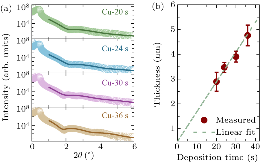
Following these analyses, the plot of the total thickness of Cu ultra-thin films against the sputtering time is displayed in Fig. 5(b). The linear fitting process reveals that the estimated thickness is almost directly proportional to the deposition time, suggesting a relatively consistent deposition rate and validating the reliability of the thickness estimates. Consequently, the sputtering durations of 20 s, 24 s, 30 s, and 36 s yield ultra-thin Cu films with average thicknesses of 2.893 nm, 3.472 nm, 3.936 nm, and 4.761 nm, respectively.
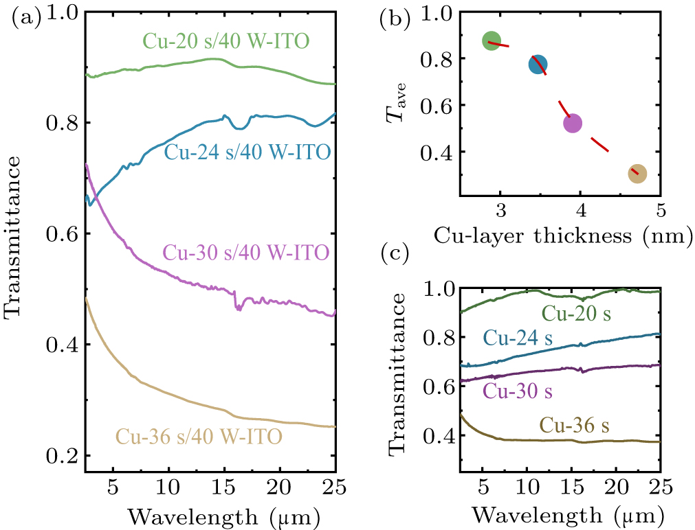
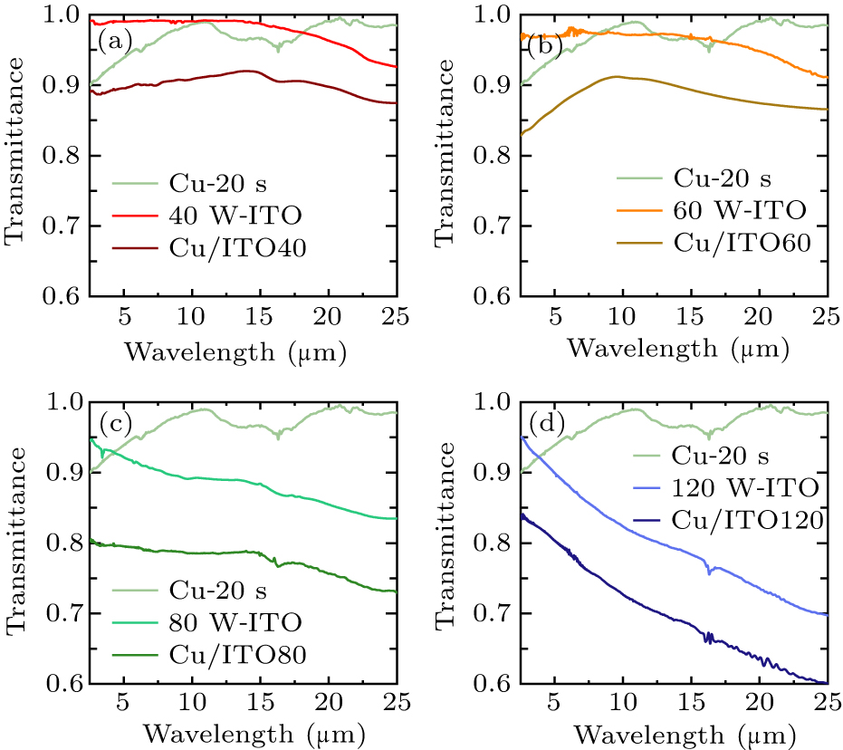
The transmittance spectra of Cu/40 W-ITO films with various Cu capping layer thicknesses are presented in Fig. 6(a). The average infrared transmittance of Cu/40 W-ITO films is also calculated using Eq. (2), as shown in Fig. 6(b). A pronounced decrease in average infrared transmittance is observed with the increase of Cu capping layer thickness. To investigate the origin of this dependence, we performed infrared transmittance measurements on monolayer Cu films deposited on KBr substrates, displayed in Fig. 6(c). It is found that the infrared transmittance of the monolayer Cu films declines significantly with increasing thickness, resulting in reduced infrared transmittance in Cu/40 W-ITO bilayered films with thicker Cu capping layers. We also note that the Cu-36 s sample exhibits characteristic Drude-like metallic behavior,[75] manifested by a monotonic decrease in infrared transmittance with increasing wavelength. As an opposing scenario, the observed positive correlation between the infrared transmittance and wavelength in Cu-20 s, Cu-24 s, and Cu-30 s films arises from the formation of metallic islands during the initial stages of thin film nucleation.[76] Thus, the crossover in the spectral slope reveals that a thickness-driven structural transition[77] from isolated island growth to a continuous bulk-like phase occurs with increasing film thickness, which is consistent with our findings from XRR measurements. It can be inferred that the formation of continuous layered structures further enhances the interaction between infrared electromagnetic waves and the film structure,[42] leading to enhanced infrared reflectivity[78] and reduced transmittance.
The measured sheet resistance of Cu/40 W-ITO films is plotted versus the Cu capping layer thickness in Fig. 7(a). It is found that the sheet resistance (less than 500 Ω/sq) of Cu/40 W-ITO films is drastically lower than that of the bottom ITO layer (∼ 10,000 Ω/sq), demonstrating that the introduction of an ultra-thin Cu capping layer significantly enhances the overall electrical conductivity. Furthermore, it is discovered that the sheet resistance of Cu/40 W-ITO samples decreases sharply with increasing Cu capping layer thicknesses. As the capping layer thickness rises from ∼ 2.9 nm to ∼ 4.8 nm, the sheet resistance drops by nearly 90%, reaching ∼ 40 Ω/sq. Given the poor conductivity of the ITO bottom layer, this finding indicates that the resistivity of the ultra-thin Cu layer decreases significantly as its thickness increases. Combined with our spectroscopic measurements, the structural transition from an island-like structure to a continuous morphology appears to be a key factor in the enhancement of electrical conductivity of ultra-thin Cu layers. The increase in the Cu layer thickness facilitates the filling of voids between isolated islands. Consequently, the scattering of conduction electrons at surfaces and grain boundaries is thereby suppressed, leading to a reduction in electrical resistivity.[79]
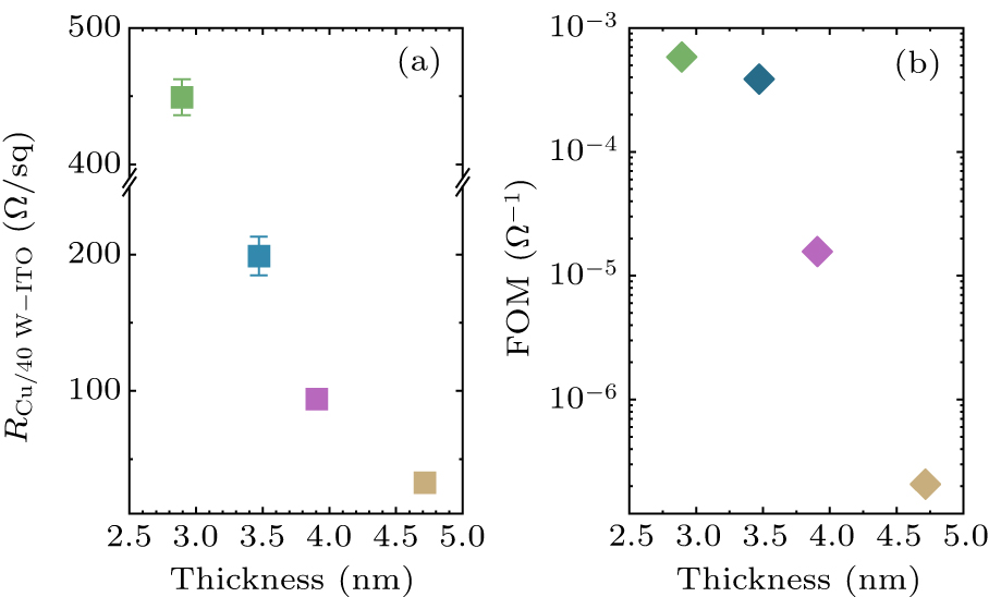
Collectively, the introduction of a Cu capping layer significantly boosts the overall electrical conductivity of ITO systems, while inducing a reduction in the total infrared transmittance, with this effect becoming progressively more pronounced as the Cu capping layer thickness increases. To determine the optimal capping layer thickness, the FOM values of Cu/40 W-ITO films are calculated using Eq. (3), with results depicted in Fig. 7(b). It is observed that the Cu-20 s/40 W-ITO film with a Cu capping layer thickness of ∼ 3 nm exhibits the highest FOM value (5.82 × 10⁻⁴ Ω−1), which is also higher than that of the pristine 40 W-ITO film (< 1 × 10⁻⁴ Ω−1). Therefore, compared to the pristine ITO samples, the introduction of a ∼ 3-nm-thick Cu capping layer enhances the overall electrical conductivity while minimizing the transmittance loss.
-
In the Cu/ITO bilayered thin films discussed below, the deposition time of the Cu layer is fixed at 20 s to ensure a thickness of approximately 3 nm, while the ITO bottom layers are fabricated with deposition parameters respectively corresponding to 40 W-ITO, 60 W-ITO, 80 W-ITO, and 120 W-ITO. The obtained Cu/ITO samples are labeled as Cu/ITO40, Cu/ITO60, Cu/ITO80, and Cu/ITO120, respectively.
As shown in Fig. 8, the introduction of the Cu capping layer results in a consistent decrease in the infrared transmittance of ITO films with varying oxygen vacancy contents. The Cu/ITO bilayered film exhibits more complex wavelength-dependent transmittance characteristics, with measured values slightly lower than the product of the transmittances of the individual 3-nm-thick Cu capping layer and the ITO bottom layer, which can be attributed to interfacial absorption or defect scattering near the Cu/ITO interface. Furthermore, the infrared transmittance spectra of the Cu/ITO films presented in Fig. 8 have been extracted and summarized in Fig. 9(a) to illustrate the impact of oxygen vacancy content on the infrared transparency of Cu/ITO films. It is found that the enhanced oxygen vacancy content in the ITO layer is correlated with the reduction in the infrared transmittance of Cu/ITO bilayered films. The average infrared transmittance values of Cu/ITO40, Cu/ITO60, Cu/ITO80, and Cu/ITO120 films are calculated to be 0.874, 0.861, 0.776, and 0.701, respectively.
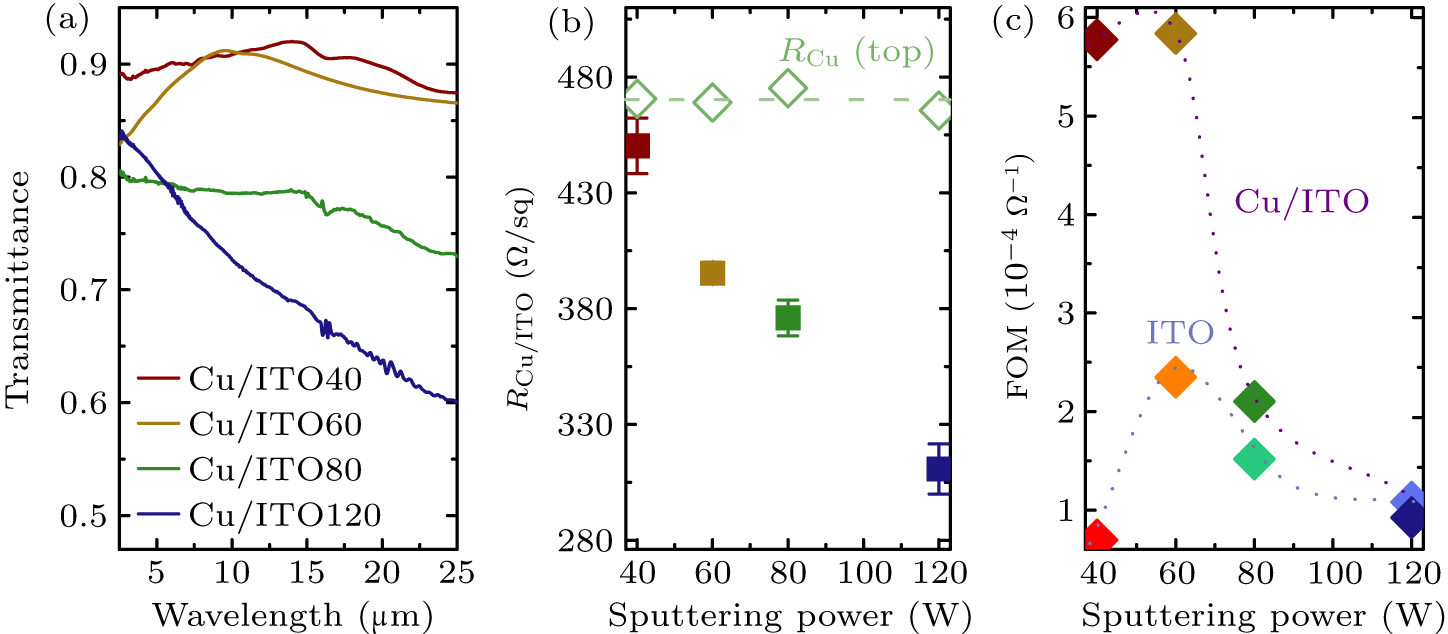
As illustrated in Fig. 9(b), the sheet resistance of Cu (3 nm)/ITO films with varying oxygen vacancy contents consistently falls within the range of 200 Ω/sq to 500 Ω/sq, demonstrating a significant reduction compared to that of pristine ITO film. This empirical evidence confirms that the introduction of a Cu capping layer improves the overall electrical conductivity, consistent with the findings presented in Subsection 3.2. Furthermore, a monotonic decrease in the total sheet resistance of the Cu (3 nm)/ITO structure has been observed as the oxygen vacancy content increases. Thus, it may be reasonably inferred that, in the absence of significant interfacial effects, the sheet resistance of Cu/ITO bilayered films (RCu/ITO) arises from the parallel connection of the Cu capping layer (RCu(top)) and the ITO layer (RITO), as described by
Consequently, the trend of (RCu(top)) values is extracted through analysis of the RCu/ITO data and the RITO values (Fig. 3(c)). Figure 9(b) demonstrates a highly consistent sheet resistance (∼ 470 Ω/sq) for the 3-nm-thick Cu capping layer, confirming its parallel connection with the ITO bottom layer.
According to these findings, we also calculate the FOM values of Cu (3 nm)/ITO bilayered films and compare them with those of pristine ITO films, as shown in Fig. 9(c). Through comparative analysis of Cu/ITO bilayered systems with varying oxygen vacancy contents, it is found that when the ITO layer possesses relatively low oxygen vacancy content (e.g., Cu/ITO40 and Cu/ITO60), the introduction of a Cu capping layer significantly enhances the overall optoelectronic performance of the films via parallel conductive mechanisms, with the FOM value doubling compared to the pristine ITO films. The Cu/ITO60 sample demonstrates the optimal FOM value, characterized by an average infrared transmittance of 0.861 and a sheet resistance of ∼ 400 Ω/sq. The moderate oxygen vacancy content within the Cu/ITO60 sample maintains high infrared transmittance in the ITO layer while improving its electrical conductivity, forming an interconnected conductive network with the Cu capping layer. However, when the oxygen vacancy content becomes somewhat excessive (e.g., Cu/ITO80 and Cu/ITO120), the intrinsic sheet resistance of ITO layers drops below 2000 Ω/sq, drastically diminishing the parallel conductive contribution from the Cu capping layer. Concurrently, transmittance losses induced by the Cu capping layer dominate and weaken the FOM enhancement.
Therefore, it can be concluded that the combined effects of the introduction of a 3-nm-thick Cu capping layer and moderate oxygen vacancy content in Cu/ITO systems can effectively improve the infrared optoelectronic performance by balancing the trade-off between carrier transport and infrared transparency. Precise control of the Cu capping layer thickness and oxygen vacancy effectively minimizes optical reflection and absorption at both the individual film layers and their interfaces. Furthermore, the introduction of the Cu capping layer optimizes the conduction paths within the bilayered film and forms a parallel conductive network with the ITO bottom layer. Notably, the Cu capping layer in the Cu/ITO structure demonstrates enhanced conductivity in comparison to the 3-nm-thick Cu monolayer previously reported in the literature.[9,80] This improvement might be attributed to the presence of the ITO bottom layer, which is capable of enhancing the adhesion of the metal layer and tailoring its microstructure, thereby improving its electrical performance.[81] These results imply a non-trivial interaction mechanism between the Cu capping layer and ITO bottom layer, highlighting the need for further investigation.
3.1. The effect of oxygen vacancy content in pristine ITO films
3.2. The effect of ultra-thin Cu capping layer
3.3. The effect of oxygen vacancy content in Cu (3 nm)/ITO films
-
In conclusion, a critical performance breakthrough in ITO-based infrared-transparent conductive films has been achieved through oxygen vacancy content modulation in the ITO layer and the strategic introduction of an ultra-thin Cu capping layer. The results demonstrate that a moderate oxygen vacancy concentration in pristine ITO films maintains an average infrared transmittance of 0.961 while reducing the sheet resistance to ∼ 2800 Ω/sq. Simultaneously, the infrared optoelectronic performance of Cu/ITO films exhibits a strong dependence on the thickness of the Cu capping layer, with an optimal thickness of ∼ 3 nm. Based on these findings, the engineered Cu (3 nm)/ITO (20 nm) bilayered architecture achieves a breakthrough balance of high infrared transmittance (0.861) and low sheet resistance of 400 Ω/sq through the combined effect of the oxygen vacancy and the introduction of Cu capping layers. Preliminary studies reveal that the combined effect between the moderate oxygen vacancy concentration and the ultra-thin Cu capping layer enhances electrical conductivity via parallel conductive network formation while maintaining the infrared transmittance through the optimized thickness of the Cu capping layer and suppressed interfacial infrared light scattering losses. The metal/oxide heterostructure engineering strategy combined with defect-state gradient control has developed a novel film system with key parameters (infrared transmittance >0.80, sheet resistance ∼ 400 Ω/sq) that preliminarily meets the practical requirements for infrared-transparent conductors. Further optimization of magnetron sputtering processes and precise oxygen vacancy modulation methods will unlock substantial industrial application potential in areas such as infrared sensors, intelligent thermal control, and photovoltaic devices.
 DownLoad: