
 首页
首页 登录
登录 注册
注册


-
At temperatures above absolute zero, any substance emits electromagnetic radiation due to the irregular movement of its internal molecules and atoms. In this context, infrared detectors capture information that visible detectors are unable to capture. Short-wave infrared detection has long played a significant role in many fields. For instance, its integration with intelligent agriculture is a key application, facilitating tasks such as detecting agricultural product damage[1] and sorting damaged or foreign materials[2]. Moreover, short-wave infrared detection finds applications in night vision, fire control, and medical imaging[3, 4]. Since infrared detection technology has observed development specifically relating to military and civilian areas[5], high-performance short-wavelength infrared photodetectors have emerged, leveraging materials such as HgCdTe (MCT) and InGaAs/InP[6, 7]. The short-wave detectors of these two material systems demonstrate excellent performance. Compared with traditional MCT infrared detectors[8], devices based on antimonide (Sb) materials have garnered considerable attention for their superior function, including reduced weight, smaller size, and lower cost. On the other hand, the larger substrate size[9] along with its compatibility with array technology, presents a wide range of potential applications[10].
There are two types of photodiodes: mesa and planar structures. Mesa structures are susceptible to surface leakage current, primarily due to the presence of mesa side walls, which significantly impact device performance. In contrast, planar PN junctions mitigate this issue. Planar structure photodetectors exhibit reduced dependency on surface treatment and passivation, simplifying the process of fabrication and lowering the cost of the detectors[11]. Additionally, antimonide substrates have enabled the growth of 6-inch substrates[12]. Using the planar junction process allows for the production of low-cost, large-array detectors without the need for material epitaxy.
Both ion implantation and high-temperature diffusion ovens are employed to create P-type doped regions[13]. Previous research suggests that thermal diffusion results in lower surface damage. In this study, high-performance planar structure photodiodes were fabricated on GaSb substrates. The research focuses on thermal diffusion experiments using Zn elements. Device performance is characterized through secondary ion mass spectrometry (SIMS) tests, surface morphology assessments, and photoelectric signal evaluations.
-
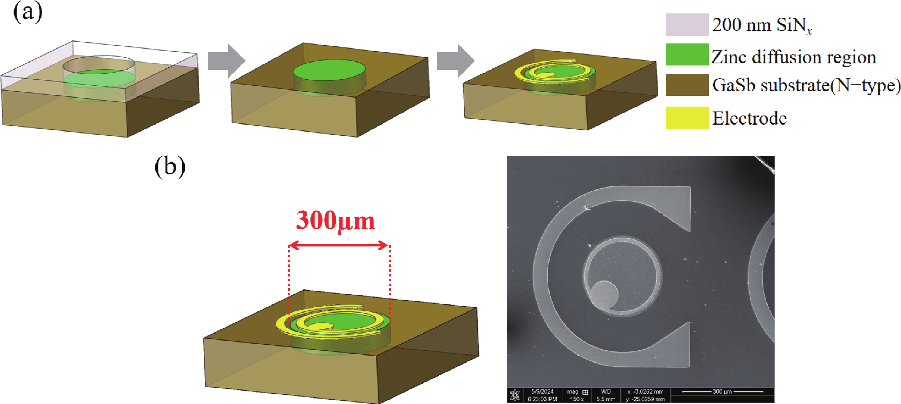
The chemical vapor deposition method was used to grow a 200 nm thickness of SiNx layer on the N-type GaSb substrate which acted as a mask to separate non-diffusion areas[14]. Numerous experiments have validated that area-selective diffusion can mitigate edge leakage current and enhance performance[15]. The selected diffusion areas were created via inductively coupled plasma (ICP) dry etching. Following surface cleaning with acetone and anhydrous ethanol, hydrochloric acid was applied to remove surface oxide. Finally, the Zn source was used as the thermal diffusion source, as shown in Fig. 1. Residual SiNx was etched using buffer oxide etch (BOE) to expose the substrate for electrode fabrication. Electrodes were fabricated through sputtering Ti/Pt/Au. The signal output of the subsequent test was obtained from the bonding pad. Fig. 1 illustrates the structure of the planner junction devices and the SEM diagram of fabricated devices.
-
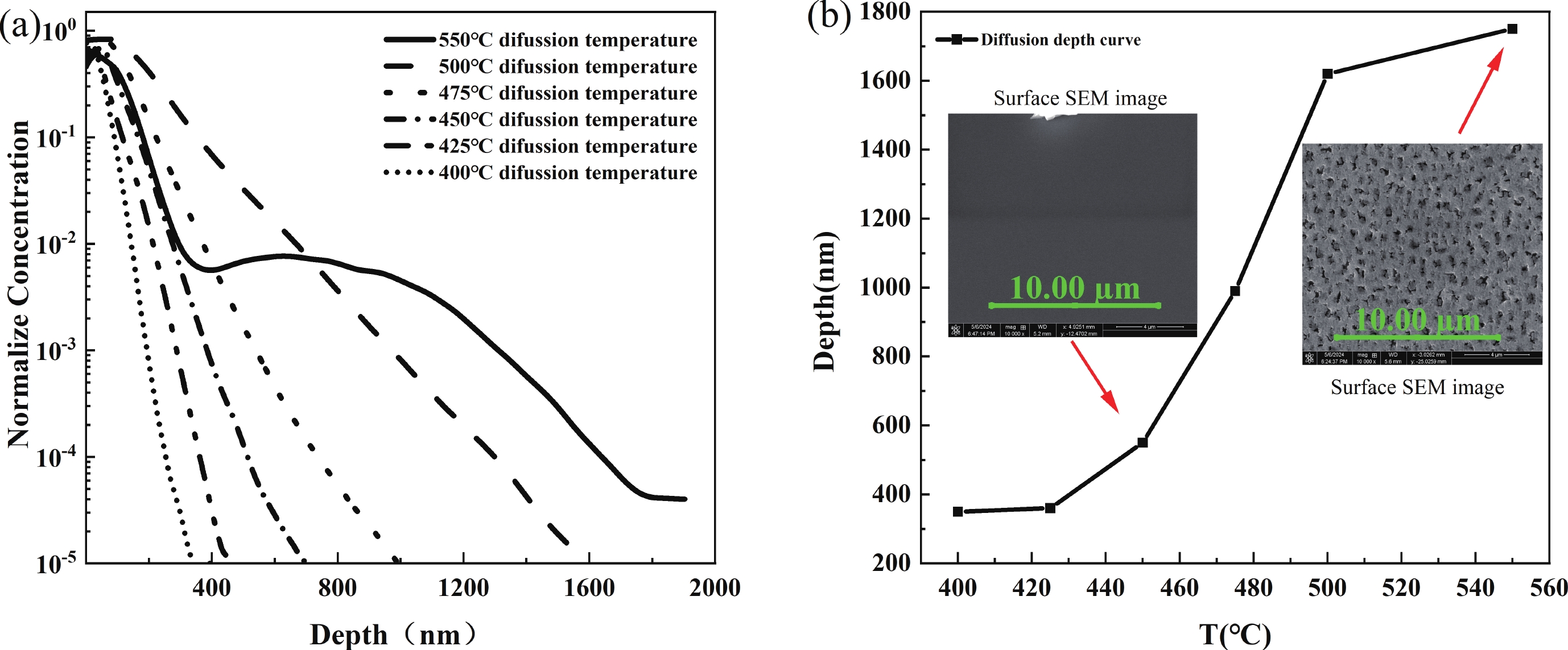
The doping curve was measured using SIMS[16]. The estimated diffusion depths ranged from 350 to 1750 nm as the diffusion temperature increased from 400 to 550 °C, as illustrated in Fig. 2(a). The diffusion depth exhibited greater sensitivity to changes in temperature between 420 and 500 °C. At lower diffusion temperatures, it was challenging for Zn atoms to diffuse into the lattice. In contrast, excessively high diffusion temperatures not only failed to increase the diffusion depth further but also led to surface damage of the GaSb material, as shown in Fig. 2(b). Fig. 3 is the cross-section TEM image and mapping energy spectrum of fabricated planar PN junction detector, the distribution of Zn atoms can be clearly seen in the diagram.
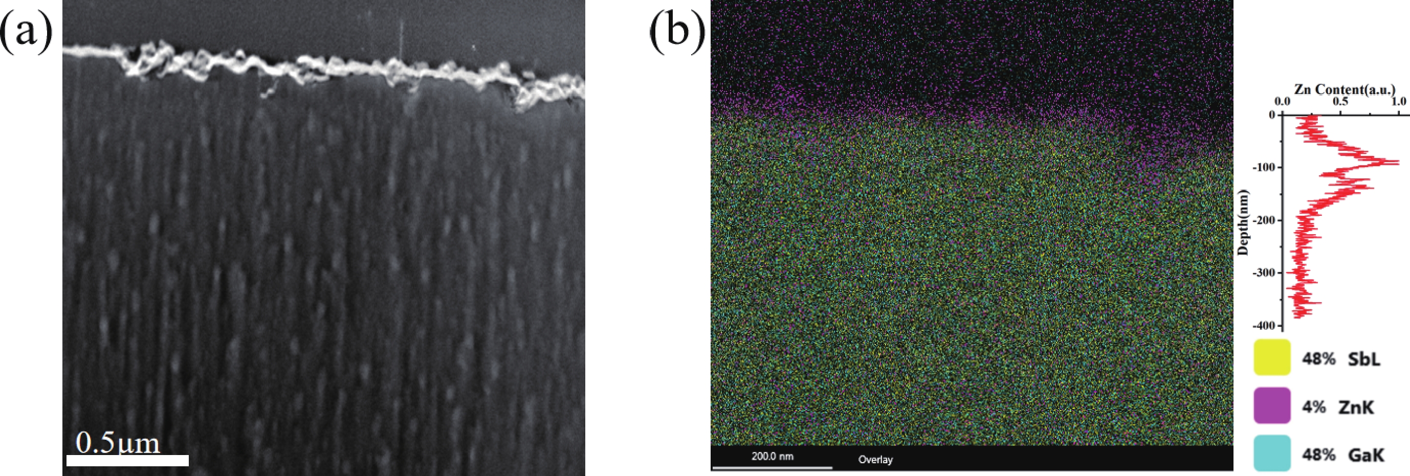
The contrast of Zn diffusion region in HAADF dark field image was not enough to distinguish the diffusion region in Fig. 3(a). However, Zn element can be obviously observed in EDS spectrum in Fig. 3(b). The red line was the relationship between normalized diffusion concentration and diffusion depth. The zero-point started from the surface of sample. After that, we simulated the energy band gaps of 450 and 550 °C devices, as shown in Fig. 4.
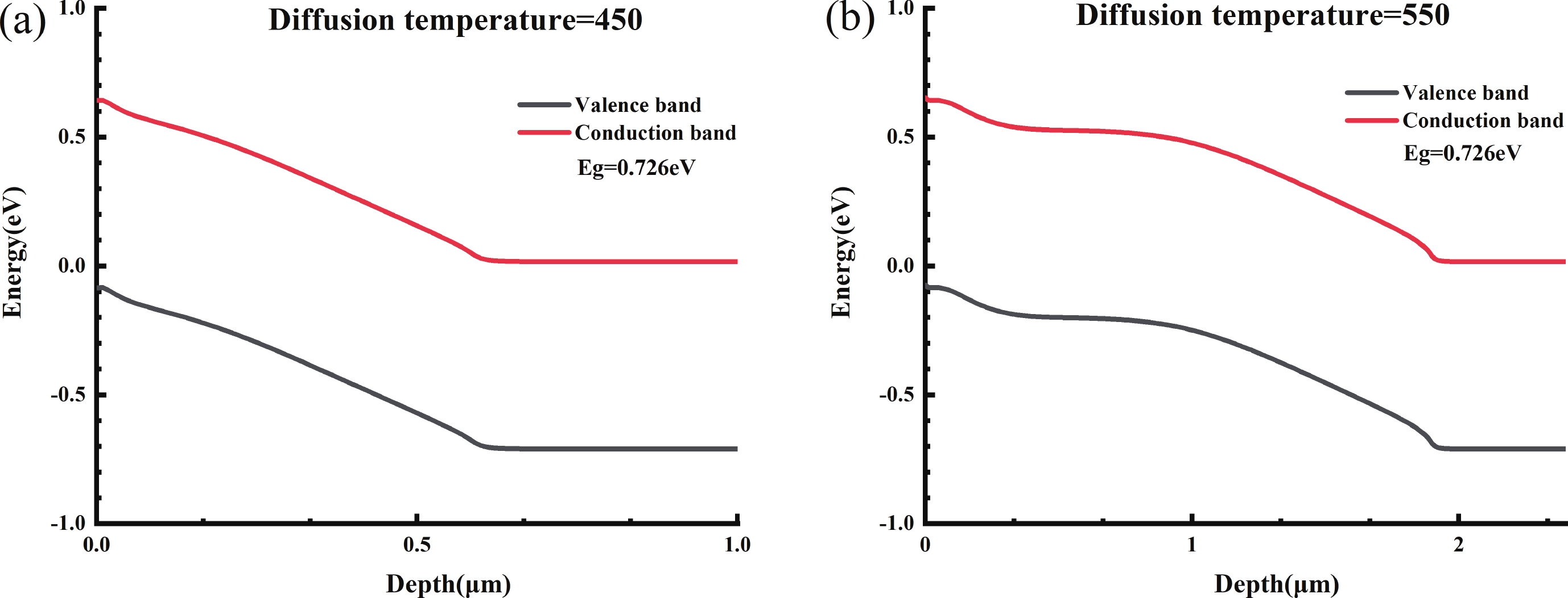
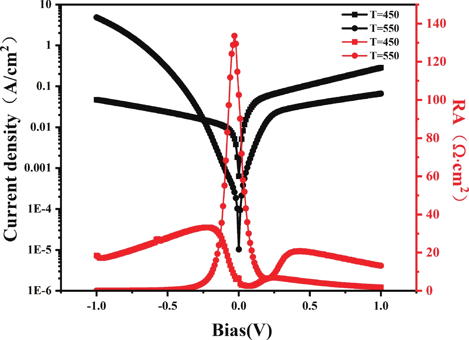
The device performance was tested through I−V measurements, Fourier transform infrared spectrometer (FTIR), and black body radiometer. Fig. 5 depicts the relationship between dark current density/differential resistance area product and bias for two devices of 700 μm diameter at room temperature. Fig. 6 shows the dark current mechanism at various test temperatures. At a bias of 0 mV, the dark current density was 1.02 × 10⁻⁵ A/cm2, with R0A at 133.5 Ω·cm2 for a diffusion temperature of 550 °C. For a diffusion temperature of 450 °C, the dark current density was 6.3 × 10⁻⁴ A/cm2 at 0 mV bias, with R0A at 30.3 Ω·cm2. The device fabricated at 550 °C diffusion temperature performed approximately ten times better than the 450 °C sample. It can be seen from the band gap diagram that moderately increasing the doping concentration helped to reduce the diffusion current and depletion region current, thereby reducing the dark current of the device[17].
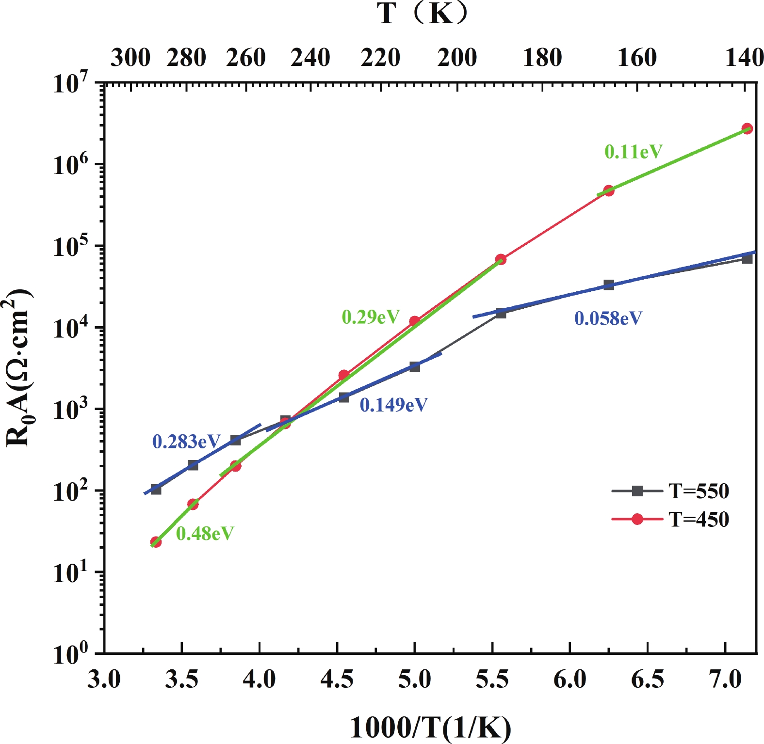
The main dark current mechanism observed in the sample diffused at 550 °C was constrained by both the generation-recombination and tunneling mechanisms (ΔE < Eg/2). At 300−260 K, the activation energy was ΔE = 0.283 eV; at 240−200 K, it was ΔE = 0.149 eV; and at 180−140 K, it was ΔE = 0.058 eV. However, at 300−280 K, the activation energy of the 450 °C diffused sample is ΔE = 0.48 eV (ΔE > Eg/2), indicating that the Shockley−Read−Hall (SHR) generation, recombination, and diffusion currents were the primary contributors to the dark current. The dark current mechanism of this set of devices at 300 K verified the results of the band gap analysis. Furthermore, the mechanisms observed at 260 to 180 K and 160 to 140 K were a combination of generation-recombination and tunneling currents. To calculate the activation energy, we followed the slope of the fitted curve (−ΔE/KBT), where KB represents Boltzmann constant.
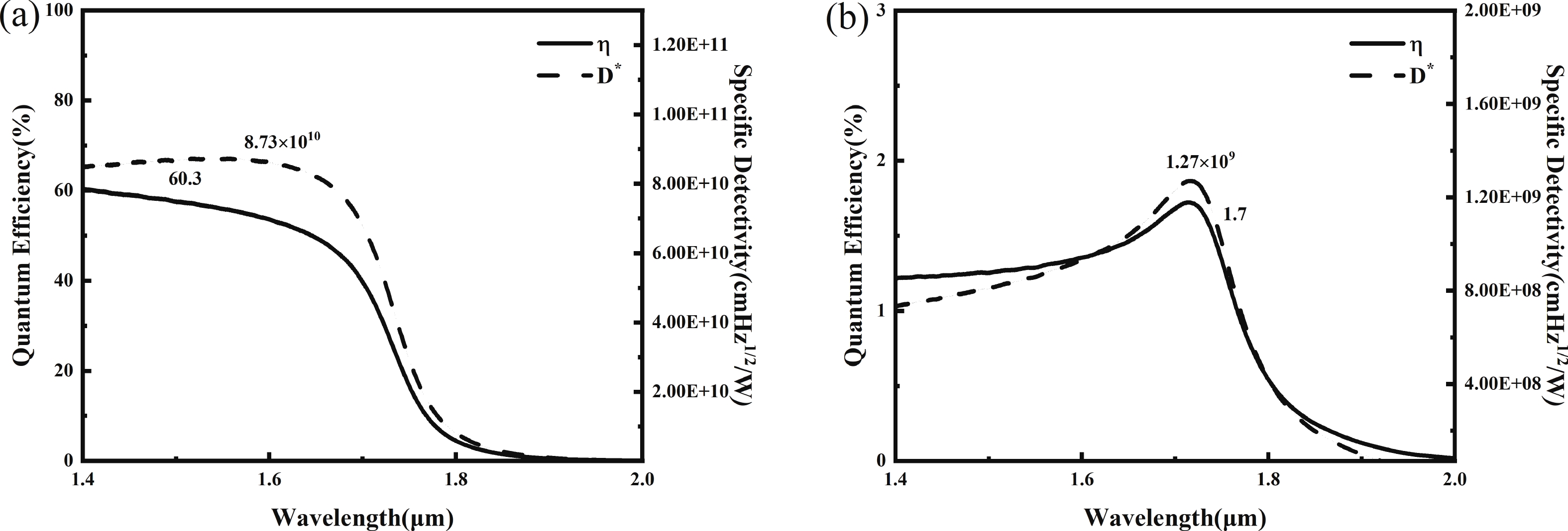
The quantum efficiency (η) and specific detectivity (D*) were measured through FTIR and black body infrared radiation tests. These parameters reflect the device's ability to generate photo-generated charge carriers and its detection capability.
Fig. 7(a) shows the performance curve and wavelength of the photodiode fabricated with a diffusion temperature of 550 °C. The maximum quantum efficiency reached 60.3%, with the maximum specific detectivity at 8.73 × 1010 cm·Hz1/2/W at 1.54 µm. These values indicate that the device has achieved an imageable level, signifying the feasibility of fabricating focal plane chips and other complex devices using this method. Additionally, due to the red-shift observed during room temperature testing, the actual 50% cut-off wavelength is approximately 1.73 μm. Fig. 7(b) illustrates the performance curve and wavelength of the photodiode fabricated with a diffusion temperature of 450 °C. Here, the maximum quantum efficiency was only 1.7%, with the maximum specific detectivity at only 1.27 × 109 cm·Hz1/2/W.
Finally, the performance comparison of the planar junction detectors is summarized in Table 1. The device fabricated with a diffusion temperature of 550 °C exhibited superior performance due to its greater PN junction depth. However, the sample diffused at 450 °C failed to meet expectations due to the short diffusion time and lower temperature, potentially resulting in lower doping concentration and uneven diffusion. This issue could be addressed by increasing the diffusion time to facilitate a comparative experiment. Through repeated experiments, a stable relationship between temperature, doping, and device performance can be established.
A 320 × 256 pixel focal plane array was fabricated using the same process as the individual devices, with a diffusion temperature of 550 °C. After depositing metal and indium bumps on both the focal plane array chip and the readout integrated circuit (ROIC), they were aligned and brought into contact using a flip-chip bonding process. Subsequently, the GaSb substrate was thinned to 50 μm via chemical mechanical polishing (CMP) to facilitate back-illumination[18]. The focal plane array featured a pixel distance of 30 μm, with each photosensitive surface area measuring 25 μm to minimize pixel crosstalk. Finally, the infrared radiation imaging of an electric soldering iron and lighter flame is depicted in Fig. 8.
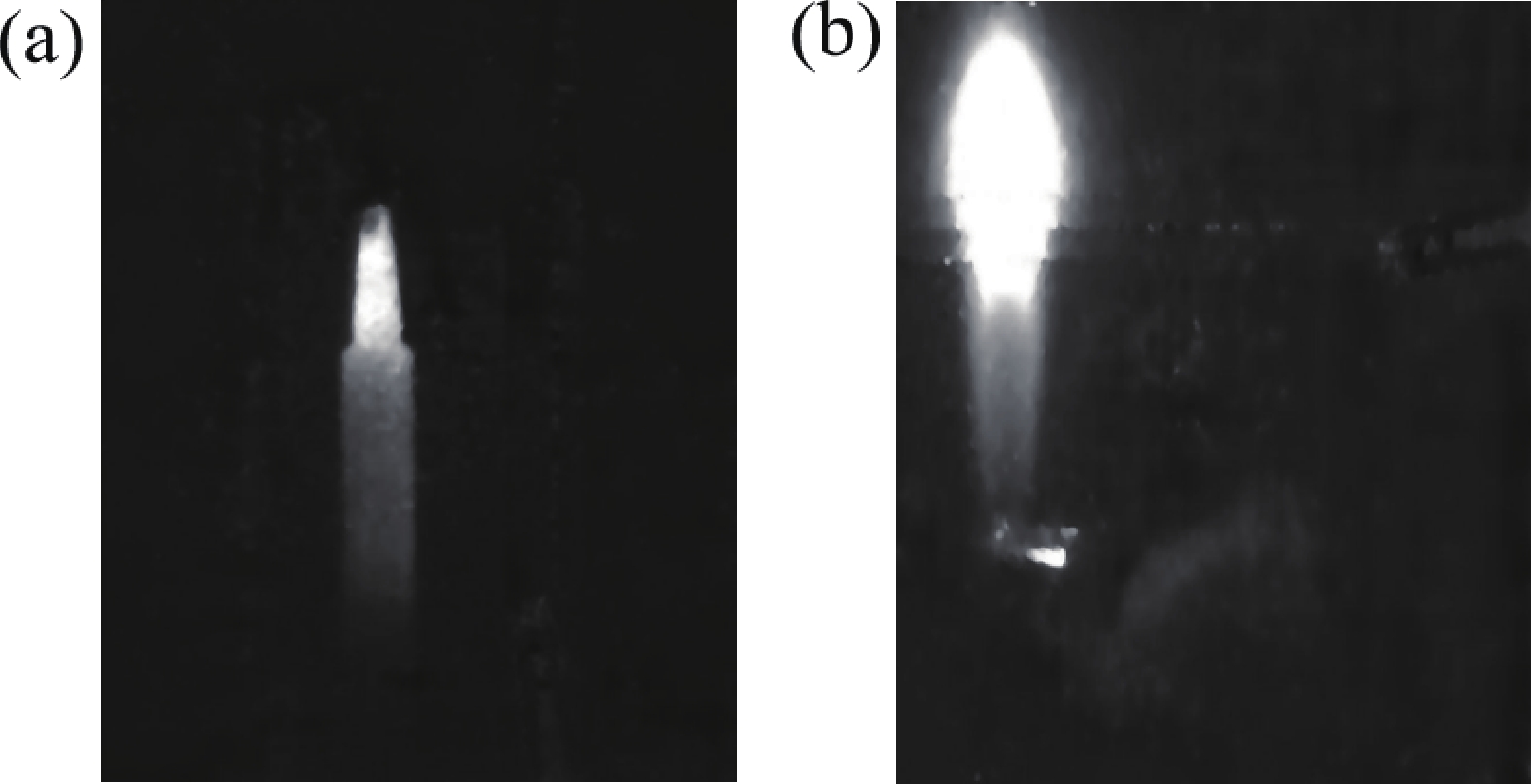
The focal plane array operates at room temperature, with a blind pixel rate of 1.25%. It exhibits excellent uniformity, performance, and stability at room temperature, demonstrating promising potential for low-cost, large focal plane arrays in the short wavelength range.
-
This paper presents high-performance GaSb short-wavelength photodiodes and focal plane arrays with a 50% cut-off wavelength of 1.73 μm at room temperature. With a diffusion temperature of 550 °C, the maximum quantum efficiency reached 60.3%, and the maximum detectivity reached 8.73 × 1010 cm·Hz1/2/W (at 1.54 μm). Our analysis indicates that the main dark current mechanism is attributed to factors other than surface leakage current, as there are no mesa sidewalls present. The dark current density was 1.02 × 10⁻⁵ A/cm2 at a bias of 0 mV, with an R0A value of 133.5 Ω·cm2. The 320 × 256 focal plane array demonstrated good imaging results and stability at room temperature. Compared to InP/InGaAs-based short-wavelength photodiodes, GaSb photodiodes can be fabricated without material deposition, suggesting promising potential for low-cost, large focal plane arrays in the short wavelength range.
High-performance GaSb planar PN junction detector
- Received Date: 16/04/2024
- Accepted Date: 21/05/2024
- Available Online: 15/09/2024
-
Key words:
- antimonide /
- short-wave infrared /
- planar junction /
- zinc diffusion
Abstract: This paper examines GaSb short-wavelength infrared detectors employing planar PN junctions. The fabrication was based on the Zn diffusion process and the diffusion temperature was optimized. Characterization revealed a 50% cut-off wavelength of 1.73 μm, a maximum detectivity of 8.73 × 1010 cm·Hz1/2/W, and a minimum dark current density of 1.02 × 10⁻⁵ A/cm2. Additionally, a maximum quantum efficiency of 60.3% was achieved. Subsequent optimization of fabrication enabled the realization of a 320 × 256 focal plane array that exhibited satisfactory imaging results. Remarkably, the GaSb planar detectors demonstrated potential in low-cost short wavelength infrared imaging, without requiring material epitaxy or deposition.
 DownLoad: