
 首页
首页 登录
登录 注册
注册


HTML
-
Deep ultraviolet (UV) detection has broad applications in the field of space communication, flame pre-warning, biomedicine, missile guidance, ozone monitoring and power system safety [1-3]. As a natural deep UV detecting material, amorphous Ga2O3 (a-Ga2O3) owns many advantages such as suitable bandgap of 4.9 eV with no need of intentional alloying, comparable photoresponsivity with its crystalline counterpart, homogeneity without crystal grains and large-area preparation at room temperature, making it a promising candidate in practical applications. [4-8] To feasibly capture ultra-weak UV light in most usage scenarios, a competent UV photodetector (PD) must possess performance with low dark current and high responsivity simultaneously, that is, high photo-to-dark current ratio (PDCR). However, the ultra-high responsivity (usually in the level of hundreds of A/W) of a-Ga2O3 UV PDs with simple metal-semiconductor-metal (MSM) structure is always accompanied by a high dark current due to the presence of abundant oxygen vacancy (VO) defects [5, 9], which is generally believed as a donor in oxide materials and a tunneling defect at the metal/semiconductor Schottky contact [10, 11]. Bottom-gate thin-film transistor architecture has been constructed to electrically deplete the electrons in a-Ga2O3 channel by a negative gate voltage, [12, 13] but the fabrication process is more complicated compared with two-terminal devices. Therefore, it is worthwhile to develop a new strategy with chemical doping of a-Ga2O3 thin films to decrease the dark current while maintaining high photocurrent using simple MSM structure.
As a stubborn residual gas in vacuum chamber, hydrogen is often unintentionally doped into semiconductor materials [14], which can greatly affect the electrical properties [15, 16]. According to hybrid functional calculations, these hydrogen atoms are considered as shallow donors and responsible for the observed n-type conductivity in
-Ga2O3 [17]. In addition, hydrogen can also compensate acceptors like gallium vacancy and improve the conductivity of -Ga2O3 [18, 19]. The above hydrogen behavior is investigated in crystalline -Ga2O3 lattice and seldom explored in the amorphous phase. Nevertheless, hydrogen in amorphous indium gallium zinc oxide (a-IGZO) has been deliberately discussed both from theoretical and experimental viewpoints, where it acts as acceptors when forming metal-hydrogen bonds and donors when forming oxygen-hydrogen bonds [20, 21]. These results suggest that hydrogen doping in a-Ga2O3 film may also modulate its electrical conductivity and further improve the device performance. In this work, intentional hydrogen-doped a-Ga2O3 films have been fabricated on quartz and polyethylene naphtholate (PEN) substrates by radio frequency (rf) magnetron sputtering technique. By in-situ tuning hydrogen flux subtly during sputtering process, the dark current of the optimal device is significantly decreased by about two orders of magnitude, exhibiting an excellent capability to detect weak UV light. In addition, flexible UV PDs on PEN substrate demonstrate great robustness in bending states and fatigue tests with comparable photoresponse as those on quartz substrate.
-
Film growth: a-Ga2O3 films with thickness of 80-100 nm were deposited on quartz (500
m thick) and PEN (125 m thick) substrates at room temperature. The substrate-target distance is about 7 cm. The sputtering target is a pure Ga2O3 material (99.99%). During deposition, no O2 gas is introduced. The quartz and PEN substrates were ultrasonically cleaned in acetone, alcohol, and deionized water successively and blown dry with nitrogen and then loaded into the growth chamber. The growth chamber was evacuated to the base pressure of 4.0 10-4 Pa before deposition. Four samples were grown on quartz substrates in a mixed atmosphere of H2:Ar = 0:10, 0.5:10, 2.0:10 and 5.0:10 sccm and named as S0, S1, S2 and S3, respectively. On PEN substrates, only one condition with H2 flux of 0.5 sccm was adopted (P1). All of the above deposition processes lasted for 15 min under a sputtering power of 60 W and a total pressure of 0.4 Pa. Device fabrication: Ga2O3 UV PDs were constructed with a coplanar MSM structure by conventional UV-lithography and lift-off technology. 100 nm ITO was deposited to form the transparent interdigital electrodes. These electrodes have 75 pairs of fingers with 5
m in width, 5 m in space and 300 m in length. Thus, the total active area is about 0.45 mm2. Material characterization: To determine the optical bandgap of these a-Ga2O3 films, transmittance spectrum was measured by using the Varian Cary 5000 UV-vis spectrophotometer. The surface morphology and roughness were evaluated by atomic force microscope (AFM, Bruker Dimension EDGE). X-ray diffractometer (XRD, Rigaku Smart Lab) was employed to confirm the amorphous nature of all the films. X-ray reflectivity (XRR) measurement was carried out on the same equipment to determine the density and thickness of all the films. Neutron reflection (NR) spectra were recorded using the non-polarized mode of multipurpose reflectometer, a time-of-flight neutron reflectometer (2.5 <
< 7 ), at China Spallation Neutron Source. The x-ray photoelectron spectroscopy (XPS, ESCALAB Xi+, ThermoFisher) was used to evaluate the chemical environment of a-Ga2O3 thin films prepared in different H2 fluxes. Device characterization: Keithley 6487 picoammeter was used to measure the dark current of all devices while Keithley 2400 was used to collect the electrical signals under light illumination. The light source was supplied by a hand-held 254 nm UV lamp. Photoresponsivity measurements were performed using a UV-enhanced Xenon lamp equipped with a monochromator, where optical power density is calibrated by a standard Si PD (Zolix).
-
As exhibited in figure 1(a), all the samples on quartz substrates show a high transmittance over 85% above 300 nm and a strong UV absorption below 250 nm. The variation of optical bandgap is shown in the inset of figure 1(a), indicating an ignorable influence of hydrogen content on the bandgap and an excellent capability of UV light detection. The AFM image of sample S1 is shown in figure 1(b) with the root mean square roughness of 0.425 nm. The incorporation of hydrogen does not degrade the surface morphology apparently compared with the pure a-Ga2O3 as displayed in figure S1. Figure 1(c) shows the grazing incident XRD curves of all the samples. No signature peak is observed except a wide envelope at 21.5, implying these thin films are amorphous without long-range order. In order to further explore the quality of the films, XRR measurement was carried out. By fitting the XRR experimental curves (figure 1(d)), the thickness as well as the mass density are determined as 84 nm/4.75 g cm-3, 85 nm/5.34 g cm-3, 93 nm/5.12 g cm-3 and 95 nm/4.80 g cm-3 for S0-S3, respectively. It can be found that the film density decreases while the thickness increases as the hydrogen flux rises from S1 to S3, implying that the in-situ hydrogen doping may change the local arrangement of atoms and cause an expansion of the nearest bond length in a-Ga2O3.
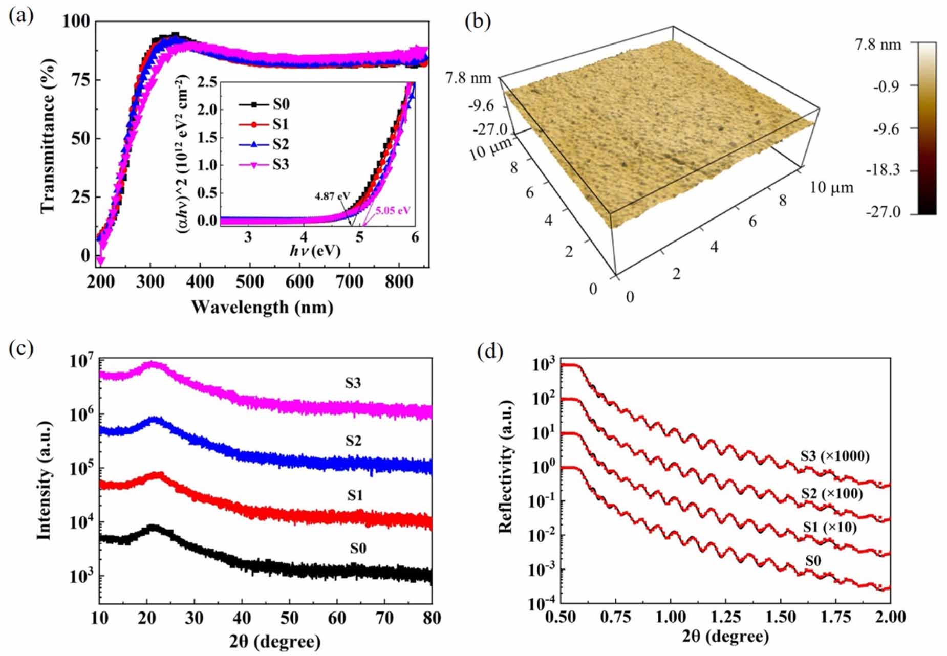
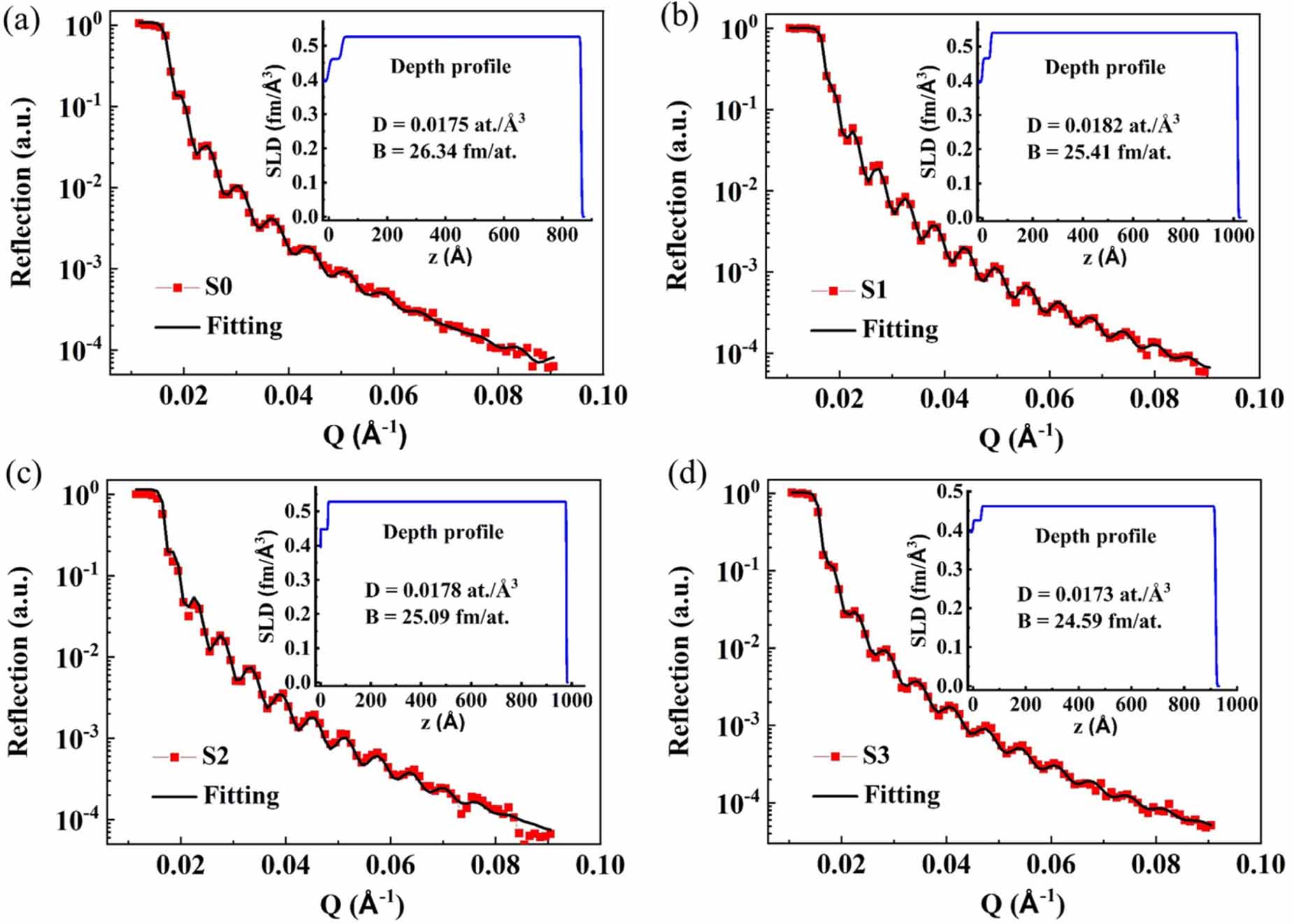
A two-layer model, including the interfacial transition layer and the main layer, was used to fit the experimental NR curves. This model is consistent with the nucleation process of physical vapor deposition, yielding the best fitting curves with uniform SLD values in the main layer and steep steps at the interface as shown in figure 2. It can be found that the value of B gradually decreases with the increase of hydrogen fluxes, indicating that hydrogen is effectively incorporated into the films, agreeing well with secondary ion mass spectrometry result shown in figure S2. It should be emphasized that even though there is no intentional hydrogen doping, the value of B for S0 is still lower than the standard value (31.985) for stoichiometric Ga2O3, which probably due to the presence of VO defects in oxide thin films. [5] In addition, the value of D also decreases as the hydrogen flux increases, consistent with the XRR results shown in figure 1(c).
Based on the above thin films, UV PDs with simple MSM structure were fabricated to evaluate the impact of hydrogen on the photoresponse behavior. Figure 3(a) shows the I-V curves of the PDs in dark and under 254 nm UV light illumination. It can be clearly found that the photocurrent of S1 enhances several times while the dark current decreases nearly two orders of magnitude compared with S0, leading to a PDCR value larger than 107. This behavior is quite different with the fact that both the dark current and photocurrent will decrease simultaneously if only the interfacial barrier height is enhanced according to previous reports where oxygen gas is introduced [5, 10]. More carriers must be excited into the conduction band. Since the bandgap is almost unchanged by hydrogen doping (figure 1(a)), the most probable origin of the extra carriers should come from the sub-bandgap states. However, the response speed does not change significantly as shown in figure 3(b), further implying the existence of abundant deep level traps. Therefore, the improvement of the photocurrent is tentatively ascribed to the new sub-bandgap states related with hydrogen doping.
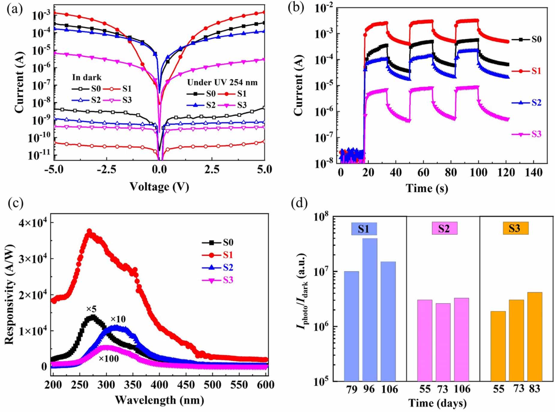
Photoresponse spectra of all samples are recorded as shown in figure 3(c). Take the best sample S1 as an example. Its responsivity is as high as 3.20 104 A W-1 at around 254 nm, corresponding to the EQE of 1.57 107% and D of 5.28 1015 Jones, respectively. Such a high detectivity is attributed to the ultrahigh responsivity and ultralow dark current of the H-doped a-Ga2O3 UV PDs. In addition, the broadband photoresponse with a redshift of the peak position is observed even though the bandgap does not change a lot according to the transmittance spectra (figure 1(a)). The response from the longer wavelength should come from the excitation of the sub-bandgap states and band tails due to the presence of abundant defects and absence of long-range order. This phenomenon has been reported in a-IGZO and a-Ga2O3 thin films previously [4, 25].
Further, to investigate the stability of the devices, a long-term follow-up test of about 3 months was carried out. All devices are placed in the drying cabinet without any passivation or encapsulation treatments. From figure 3(d), it can be seen that the PDCR values of all the devices are maintained at the original level with a slight decrease after about 100 d, ensuring a long-term service of the H-doped a-Ga2O3 UV PDs.
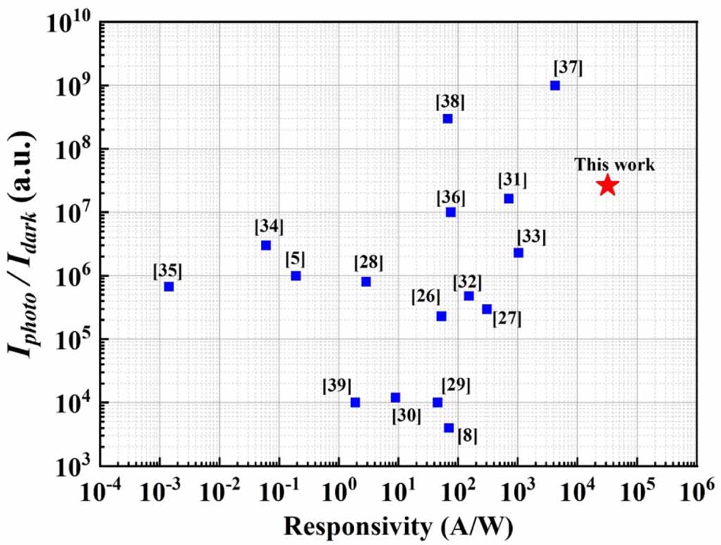
The parameters of all the representative devices on sample S0-S3 are summarized in table 1. With the increase of hydrogen flux, the dark currents show a trend of first decreasing and then increasing while the photocurrents show an opposite trend, resulting in the lowest dark current of 51.7 pA, highest photocurrent of 1.37 mA and highest PDCR value of 2.65 107 for sample S1. Therefore, a moderate hydrogen content can effectively improve the device performance. A comparison of the photoresponse parameters with previously reported Ga2O3-based UV PDs is demonstrated in figure 4. Our a-Ga2O3 PD (S1) shows an ultra-high PDCR and responsivity simultaneously, surpassing most of the ever-reported results.
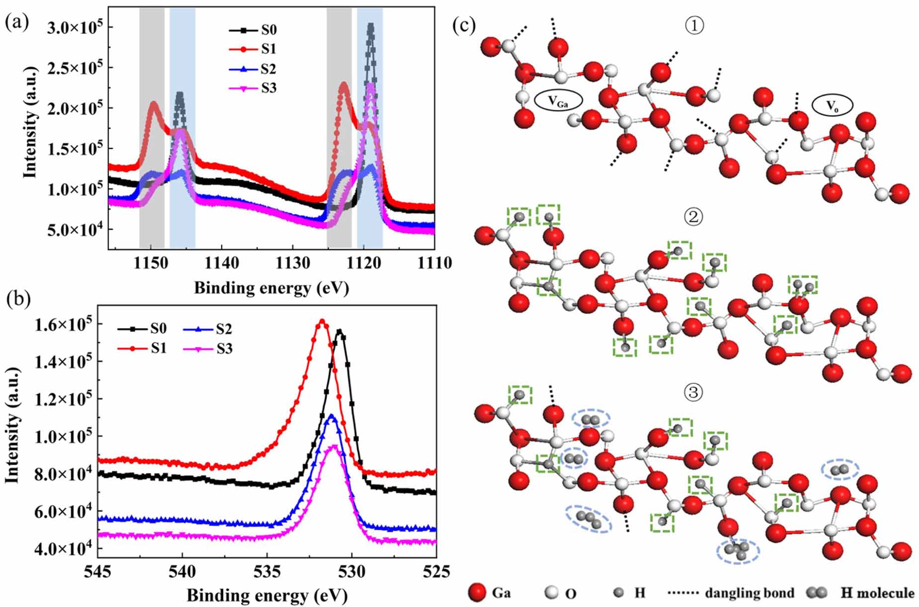
To better understand the influence of hydrogen doping on the device performance, XPS measurement was carried out. Figure 5 shows the core level spectra of Ga 2p and O 1s after calibration with C 1s peak (284.8 eV). In figure 5(a), two shoulder peaks, locating at 1149.0 eV and 1122.2 eV, appear at the high-energy side of the original Ga 2p1/2 (1145.6 eV) and Ga 2p3/2 (1119.0 eV) after hydrogen doping. Besides, the height of the shoulder peaks first increases and then decreases against the hydrogen flux, leading to the maximum value in S1. As to the O 1s curves shown in figure 5(b), the peak position changes from 530.7 eV (S0) to 531.8 eV (S1) and then moves back to 531.0 eV for S2 and S3. As previously reported, a-Ga2O3 films grown in pure Ar environment often have a nonstoichiometric Ga/O ratio with more gallium dangling bonds than oxygen [5]. Despite of that, when a small amount of hydrogen (0.5 sccm) is introduced, these dangling bonds may be passivated by the formation of Ga-H and -OH couples, making the peak position of Ga 2p and O 1s move to the higher binding energy [40]. Consequently, electrons from the dangling gallium atoms will be trapped by Ga-H bonds, leading to a lower dark current than the undoped sample S0. As the hydrogen flux increases, the radical hydrogen atoms in the plasma tend to combine with each other to form H2 molecules and escape away from the films easily, making no contribution to or even weakening the passivation of the dangling Ga/O atoms. Consequently, the number of Ga-H and -OH bonds also decreases, leading to a decrease of the shoulder peaks of Ga 2p and recovery of O 1s. A schematic diagram of the chemical bonds under different hydrogen fluxes has been shown in figure 5(c).
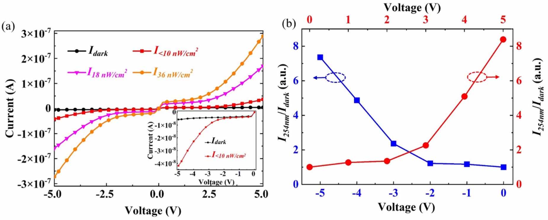
Further, photoresponse behavior under ultra-weak UV light was investigated for sample S1. Figure 6(a) shows the I-V curves in dark and under illumination of the UV 254 nm light with different intensities. The PDCR value can reach two orders of magnitude under the irradiation of a 36 nW cm-2 light source. Under the weakest light source (<10 nW cm-2), the PDCR is still nearly an order of magnitude as shown in the inset of figure 6(a). Besides, the dependence of PDCR value on the applied bias voltage under the weakest light is displayed in figure 6(b). It can be seen that the PDCR increases as the voltage increases both at the positive and negative biases. The above results indicate the great potential of our UV PDs to be applied under extremely weak light sources.
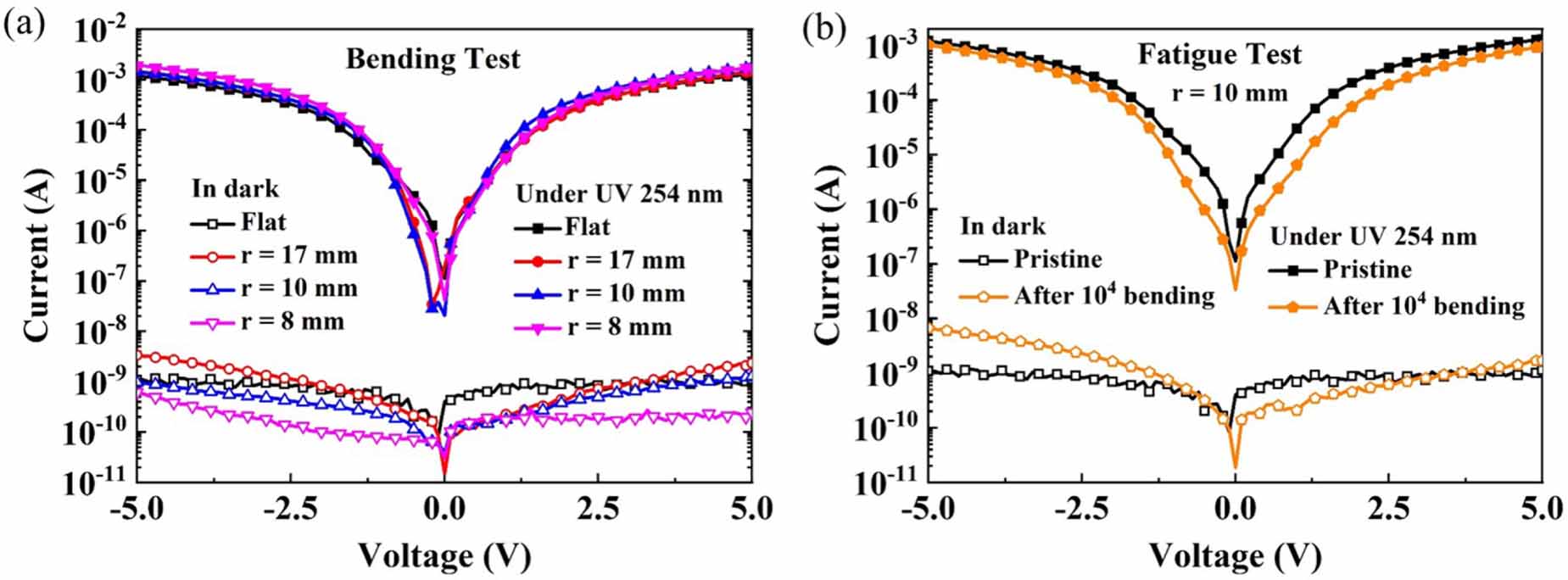
At last, H-doped a-Ga2O3 UV PD was fabricated on PEN substrate using the same preparation condition as sample S1. This sample is named as P1. To investigate the flexibility of P1, I-V curves in dark and under UV 254 nm illumination were recorded in different bending states and after multiple bending cycles. As shown in figure 7(a), P1 exhibits almost the same photocurrent at different bending radius r (r = 8, 10 and 17 mm) as the flat state. However, the dark current fluctuates nearly one order of magnitude, probably due to the varying surface tensions and probe/electrode contacts under different bending states. Figure 7(b) compares the I-V curves in flat state before and after 10000 bending cycles with r = 10 mm. Both the dark and photocurrent degrade a little bit within the tolerable range. These results indicate the robustness of flexible a-Ga2O3 UV PD, promising the potential applications in flexible optoelectronic areas.
-
In summary, by precisely adjusting the flux of hydrogen gas during magnetron sputtering process, in situ H-doped a-Ga2O3 UV PDs with excellent performance have been developed both on the rigid quartz substrate and flexible PEN substrate. Based on the combined analysis with XRR, NR and XPS, it is suggested that the prevailing VO defects in a-Ga2O3 thin films have been effectively passivated via the formation of Ga-H bonds, resulting in an obvious reduction of the dark current. The optimum device shows a remarkable detection ability under ultra-weak UV light irradiation (<10 nW cm-2), implying its potential application in various fields such as civil and national security. In addition, flexible UV PD has been achieved with the superiority of low cost, room-temperature detection, easy integration and mass production, demonstrating great prospect in flexible and transparent electronic fields.
-
In this work, hydrogen-doped a-Ga2O3 thin films and the corresponding UV PDs have been achieved with a significant decrease of the dark current, providing a new way to improve the PDCR values of a-Ga2O3 UV PDs and endowing it the capability for ultra-weak light detection. In contrast to oxygen modulation, where the dark current and photocurrent decrease simultaneously as oxygen flux increases, a new defect may form after the incorporation of hydrogen atoms, which behaves like a killer of carriers under dark and a booster of carriers under light illumination. Although a series of measurements have been carried out, understanding of this new defects is still very limited since it is not easy to characterize a-Ga2O3 thin films with wide bandgap, high resistance and random atom arrangement, not to mention that detecting hydrogen is also a tough task. More brilliant characterization method as well as theoretical calculation of amorphous oxide semiconductors with hydrogen doping are definitely quite desirable. In addition, to promote the practical application of this device, the stability investigation must be executed further.
 DownLoad: