
 首页
首页 登录
登录 注册
注册


 下载:
下载:
-
The deposition of a crystalline film over a desired area is a long-sought technique since decades ago owing to the important application in scalable micro-/nano-scale manufacturing in both the fundamental research and industrial application. This had been achieved using the stencil lithography (SL) technique for selective area deposition, which is an obsolete technique by locally shadow-masking part of the substrate surface in prior to the arrival of the material flux in the physical vapor deposition, forming a patterned film according to the feature in the stencil mask (Fig. 1). Since this mask is (semi-)rigid and mechanically strong, this technique has also been extended to material etching[1-2], ion implantation[3-4], and nano-imprint[5-6] besides film deposition. Compared with the selective area epitaxy on a pre-patterned substrate, the film quality grown using SL could be maintained since the patterning is performed on the stencil mask and the substrate is pristine, providing a deposition environment similar to a normal one. Besides, SL is compatible to the growth of all kinds of materials include metal, alloy, and multi-element compound[7-14] as well as various physical vapor deposition techniques like molecular beam epitaxy[7-8,14-15], pulsed laser deposition[10,16-18], atomic layer deposition[19-21], sputtering[22-23], etc., which exhibits powerful extension in material synthesis and device fabrication.
Materials that can harbor novel quantum effects, such as topological physics and strong correlation, have attract great attention and interest[24]. Typical examples are topological insulator[25-31], topological (Dirac and Weyl) semimetal[32-37], topological superconductor[28,38-51], 2D materials[52-54], chiral magnet[55-59], etc. The films of these materials in the 2D limit are particularly interesting, which provides an extra degree of freedom/confinement to manipulate the quantum effect. Besides, some exotic quantum effects are embedded within the hetero-interfaces as well, such as interfacial superconductivity[60-61], Dzyaloshinskii-Moriya interaction[62-63], Rashba spin–orbit coupling, magnetic proximity effect[25,64-69], etc. Keeping the interface clean and atomically sharp could maximize the wavefunction overlapping of the two constituent materials and extend the coherent phase, which results in prominent interface effects. Thus, there is an urgent need in fabricating these materials and heterostructures into micro-/nano-scale functional devices in a clean manner, aiming for the next-generation quantum technologies. However, there are some questions that need to be addressed before the practical applications. Unlike conventional semiconductors such as Si and GaAs, these quantum materials are usually not very stable even in ambient conditions. Although a protective layer can prolong the lifetime, it not only complicates the device fabrication like etching the film to a specific geometry but also hinders the fabrication of electrical contacts. To improve the device performance, simplifying the fabrication process and especially minimizing the time exposing the sample to ambient conditions while keeping the film crystalline quality become extremely necessary.
One of the possible approaches to solve these problems may refer to the in-situ device fabrication using the SL. By using the SL in various physical vapor depositions, not only the film and heterostructure can be selectively deposited onto the desired areas but also the electrical contacts can be fabricated in situ without breaking the vacuum, keeping all the interfaces clean and atomically sharp, minimizing the device fabrication process in ambient conditions. In this review, we rediscover the functionalities and advantages for the fabrications of quantum material devices using the SL and review the potential applications of SL in these quantum materials.
-
The preparation of the stencil mask is one of the crucial steps for SL. Depending on the demanded vacuum condition (the mask may outgas at the growth temperature) and the required resolution of the pattern, various materials could be used for constructing the mask. For example, Kovar alloy has been used for constructing the mask to sputter a patterned film[22], and refractory metal such as tantalum was used in molecular beam epitaxy-SL growth, both of which are compatible to ultra-high vacuum and can achieve hundreds of μm- to mm-size pattern. Due to the surface roughness and fluctuation, these masks cannot be machined to contact closely with the substrate surface and, hence, they only could be used if the resolution of the pattern is not critical. To address this issue, the low-stress silicon-nitride membrane and silicon wafer with extremely flat surfaces have been widely used as (semi-)rigid stencil masks, which are also compatible to ultra-high vacuum. Thanks to the mature semiconductor techniques, the feature on these masks can reach a resolution down to sub-100 nm. The silicon-nitride layer with thickness of hundreds of nm is usually deposited on a single/both surface(s) of a silicon wafer, which is an ideal material for constructing the mask in SL owing to its great thermal stability, mechanical strength, and chemical inertness. The crystalline silicon mask constructed via anisotropic etching becomes an increasingly popular choice as it allows a more robust mask structure than silicon-nitride membrane of similar thickness, which is a rapid, low-cost, and wafer-scale process[72-73]. It has been reported that masks made of both the silicon-nitride membrane and silicon wafer can achieve a finest resolution of tens of nm for patterning various metal films[9,74-76].
-
Besides the advantages reviewed by Refs[12-13], SL owns the following advantages that quantum material devices are particularly benefitted from:
-
The usual procedure for fabricating micro-/nano-scale devices, including etching the material to a specific geometry and electrode depositions, relies on techniques such as the photolithography and e-beam lithography. However, in some circumstances, it would be necessary and convenient to fabricate devices in resistless manners. Indeed this manner is equivalent to applying these resist-techniques to fabricate the small structures on stencil masks rather than directly on the substrate or material, which leaves the material and substrate pristine, that is, the SL. In this way, the material deposition processes only include the substrate, evaporated material, and the mask without any further resist, chemical solvents, energy radiation, or mechanical pressure. All the materials involved in SL-deposition could thus be carefully selected to accommodate the ultra-high vacuum. Therefore, the SL maximizes the cleanliness in material deposition and the quality of the device based on in situ fabrication. This compatibility allows the SL to be readily expanded to all of the physical vapor deposition techniques as well.
-
The stencil masks made by lithography and etching allow for the transmission of atoms, ions, or molecules from the openings to the substrates, which could not only be used in all kinds of physical vapor depositions but also the etching and ion implantation to a certain pattern. Different designated patterns and features can be reliably constructed based on the conventional micro- and nano-fabrication techniques, which could fulfil the modern development of multifunctional device structures. As the stencil mask is placed over the substrate, it can be flexibly manipulated among different fabrication processes to achieve multiplex device structures. For example, one can place the mask directly on a substrate before the deposition to achieve the selective area growth on a substrate; or after multiple continuous film depositions, the mask is then placed for the final-step metal deposition to form a heterostructure devices with electrodes; or only use the mask to deposit some pattern that is sandwiched between two continuous films, forming an embedded nanostructure at the interface between the two materials; etc. Such high flexibility and variety in both the layer structure and patterned structure showcase the power for engineering multifunctional devices.
-
The stencil mask can be removed after patterning or etching from the substrate-mask assembly and placed onto a new substrate for the next batch of use. Such a process can be reused for many times, which substantially reduces the fabrication costs and provides an efficient patterning replication using different evaporated materials onto all kinds of substrates. Long-term evaporation through the stencil mask will be accompanied by gradual clogging of the openings and apertures due to the adhesion of the evaporated materials onto the mask. However, the clogging can be fully removed by etching or ion-implantation. Moreover, to reduce the clogging, the stencil mask (particular for those with nano-scale apertures) can be coated with alkyl and perfluoroalkyl self-assembled monolayers, which were shown to considerably reduce the adhesion of the evaporated materials onto the mask[77-78]. It was reported[78] that such a coating technique can result in an increase in material deposition through the apertures by more than 100%. Therefore, the clogging is not an issue by routinely etching or the self-assembled monolayers coating, improving the performance and lifetime of the stencil mask and hence increasing the throughput of SL.
-
As stated above, most of the quantum materials are indeed not very stable even in ambient conditions. Multiple device fabrication processes can further degrade the material quality or even eliminate the quantum effect in the material. Conventional fine-scale device fabrication processes, such as coating and baking of resist and the e-beam lithography, can inevitably dope the material more or less, which modifies the position of Fermi level, while the application of high-voltage and scanning of e-beam may irreversibly destroy the crystalline structure of the material. Thus, the more complex fabrication processes, the lower the yield of device fabrication will be, either of which fails can eventually cause the malfunction of the whole device. Therefore, the device yield could be substantially increased if substituting part of the conventional fabrication processes with the SL, or even finishing the entire device fabrication using the SL only. Also, traditional patterning techniques, in particular the e-beam lithography and focused ion beam, are slow when patterning for a large area, and the patterning process needs to be repeated for every different sample, which is expensive and time-consuming. These problems limit the scalability of the devices. Instead of repeating these complex processes, the stencil mask can be made to cover the entire substrate surface and pattern the mesoscopic structures with one-time
deposition. A rigid or semi-rigid stencil mask, such as silicon wafer and silicon-nitride on silicon wafer, has been shown to be sufficiently strong to self-sustain for a large area, which enables the fabrication of mesoscopic devices on a large scale[76]. Early in 2009, it has already been reported that the SL using a silicon-nitride membrane enables to pattern sub-100 nm superconductive tunneling junction array at a full 100-mm wafer scale with 1 μm alignment resolution[79].
-
The applications of SL have been used in patterning various materials and their devices on all kinds of substrates, such as plasmonics, transistor, magnetic and superconductive mesoscopic structures, biosensor, flexible and wearable electronics, solar cells, etc., which have been covered in several other excellent reviews[12-13]. Below we only emphasize the designated applications of SL in fabricating quantum material devices.
-
As stated above, so far most of the quantum materials that are potentially applied to electronic devices applications are fabricated as thin film, especially in the 2D limit. It is known that the quantum effects of these materials are significantly affected by the electrical contacts that connect these materials with external circuitry[80]. However, it remains challenging to create high-quality electrical contacts for these thin quantum materials because several interface issues, leading to high contact resistivity and undesirable contact type[81]. As stated above, the SL can be used for in-situ growth and device fabrication without breaking the vacuum of the system. Generally, to fabricate a mesoscopic device, the resist will be commonly used in lithography processes. However, it is commonly observed that there will be some residual resist on the contact area after development before the metal deposition[82], which hinders or degrades the formation of a clean Ohm contact to the quantum materials, or increases the contact resistance. Moreover, the residue on the sample surface will contaminate the sample andcause incidental a doping effect, which locally modifies the electrochemical potential and provides extra scattering sites to the quantum material. Thus, it is believed that the residual resist is one of the causes of the bottleneck for further increasing the sample mobility. This is particularly crucial for 2D materials such as graphene, stanine, and black phosphorus that consist of only a few monolayers of atoms and, hence, very sensitive to surface contaminants. N. Staley et al. developed a lithography-free for fabricating graphene planar tunnel junction using ultrathin quartz filaments as stencil masks[83]. Possible weak localization behavior and an apparent reduction of density of states near the Fermi energy were observed. Later, W. Bao et al. improved the lithography-free technique for fabrication of clean, high quality graphene devices based on the silicon stencil masks[84]. As shown in Fig. 2(a), a 100-μm thick silicon layer was used as the stencil mask, which was patterned using e-beam lithography and inductively coupled plasma etching for depositing the electrical contacts. After aligning the resulted mask to the graphene sheet, the entire assembly was transferred into a vacuum chamber for metal deposition as shown in Fig. 2(b). It was found that the metal contacts will typically extend beyond the mask openings by ~ 0.3–0.5 μm due to the extended size of the metal source and the finite mask–device separation. Graphene devices fabricated by this technique show significantly higher mobility values than those obtained by the standard e-beam lithography. This technique has also been extended to fabricate a suspended graphene device, whose mobility can be improved to as high as 120,000 cm2/(V·s). The mask used in this study was reported to be exceedingly robust, which can be used for more than 20 times.
-
Heterostructures involving quantum materials with conventional materials usually bring about surprising quantum effects at the interfaces. To probe the effect arisen from the quantum material or how the involvement of the quantum material affects the physicochemical properties of the whole heterostructure, convincing evidences could be obtained from a control experiment that can immediately compare a sample with the quantum material and another without. However, such a control experiment may suffer from a problem that the constant variables in the experimental samples and control samples cannot be always kept precisely the same. For example, owing to the fluctuations in material deposition conditions including the flux rate, substrate temperature, surface topography, and vacuum, etc., the quality of samples varies from batch to batch more or less. This will challenge the fabrications of both samples that show the same constant variables and designated control variables. Thus, the conclusion extracted from such a control experiment could be elusive. It seems that this problem may be solved by fabricating a number of experimental and control samples, however, this approach increases the total cost and cannot fully address this problem anyway.
From this point, the SL provides another method that could solve this problem. Take the topological insulator film grown by molecular beam epitaxy-SL as an example. It was theoretically shown that the topological surface states from can act as an effective electron bath that allows oxygen and carbon monoxide molecules more prone to dissociate and get adsorbed on the surface of a noble metal/topological insulator heterostructure via enhancing the molecular adsorption energies[85]. A desired control experiment would be comparing the surface reactivities of the noble metal/topological insulator heterostructure with the noble metal film only. However, the surface reactivity may also be varied by the delicate details of the surface topographies of the substrate and the noble metal film, which also vary from sample to sample owing to the deposition conditions. Thus, fabricating two or more samples and comparing their differences may not be able to lead to a convincing conclusion. In this case, the SL could be used to address this problem by separating a single piece of substrate into two halves, which could act as the experimental and control samples respectively. In this way, the fluctuations in constant variables should be minimized. Experimentally, half the surface of a single piece of GaAs substrate was covered by a tantalum strip in situ in prior to the deposition of 7-nm topological insulator film Bi2Te3. The tantalum strip was then removed in situ to expose the entire sample surface before the deposition of a 9-nm-amorphous-Pd overlayer. In this way, the control experiment could be performed using this single piece of sample, half of which contains the Pd/Bi2Te3 heterostructure while the other half is solely the Pd film. After exposing this sample to ambient conditions, one can compare the time-of-flight secondary ion mass spectra, XPS core-level and Auger spectra of the involved elements as shown in Fig. 3. It is clear that Bi2Te3 film could enhance the adsorption of organics on the surface of Pd and the oxidation of Pd. Since Te is a congener of O and can act as an oxidizing agent for the metallic Pd, the control sample could be improved
by in situ evaporating Te (nominal thickness of 1.3 nm) onto the entire surface of the above control sample. It was found that the surface concentration of Te and the concentration ratio of Te/Pd in the region with Bi2Te3 film are substantially higher than those obtained from the region without. Therefore, by these control samples fabricated using the SL, the surface reactivity of Pd in the region Bi2Te3 film can be clearly shown to be enhanced by the underlying Bi2Te3 film.
Another example is the direct evidence of the Bi2Te3 film-induced interfacial superconductivity in FeTe based on the control sample fabricated using SL. Likewise, the experimental and control samples as shown in Fig. 4(a) are deposited onto a single substrate in order to minimize the fluctuations in constant variables. By measuring the temperature-dependent resistance curves at various regions of this sample shown in Fig. 4(b), it was found that the region fully covered with a Bi2Te3 layer shows a single superconducting transition, while the region without Bi2Te3, equivalent to a pure FeTe layer, exhibits a semiconducting behavior without any signature of superconductivity. For the middle region that consists of a Bi2Te3/FeTe heterostructure and a pure FeTe layer, the resistance curve show similar characteristics in the superconducting transition to that of the Bi2Te3/FeTe heterostructure except a different residual resistance. This residual resistance originates from the non-superconducting part in the pure FeTe layer. All these characteristics of the control sample demonstrate thatthe Bi2Te3 film is indispensable for inducing superconductivity in the Bi2Te3/FeTe heterostructure. Therefore, the SL is helpful for designing an ideal experimental and control sample that could be deposited onto a single piece of substrate. The experiments performed on such a sample could thus provide strong evidences to support the conclusion on the emergent effect.
-
Devices that could realize designated functions would be particularly benefitted from the SL in terms of, firstly, the clean interface that can dramatically enhance the interfacial coupling of the two constituent materials. Typical examples are the superconductive and magnetic proximity effects, which require atomically flat and clean interface for extended electron wavefunction overlapping and Cooper pairs tunneling. Here, the clean interface is very necessary since the phase coherence lengths in both effects are generally short, ranging from a couple of nm to about hundreds of nm even in the clean limit. If the interface is contaminated by some residual resist and adsorbate, or oxidized by the ambient air, i.e. the heterostructure is formed by some ex-situ technique, such lengths will be substantially shortened, which will diminish or fully eliminate the proximity effect. Secondly, instead of continuous thin-film heterostructures that are normally grown by various physical vapor depositions, discontinuous films and thin-film heterostructures in designated patterns and geometries can be formed using SL. In this way, specific functional devices can be realized without additional etching or deposition processes. Here, these device structures include the Hall bar, Corbino structure, tunneling junction, Josephson junction, arrays of dots and wires, etc., which are widely used and important for engineering the quantum effects.
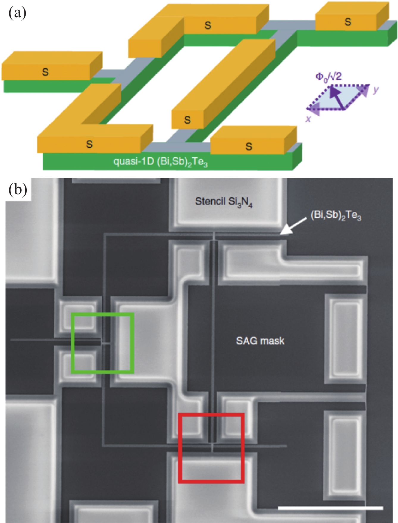
Using in-situ SL in molecular beam epitaxy, P. Schüffelgen et al. fabricated superconductor-topological insulator-superconductor Josephson junctions and networks of hybrid nanostructures. Such a device aims at the realization of superconductive proximity effect from Nb to the topological insulator, giving rise to the topological superconductor that is promising for constructing the topological qubit in quantum computation[87]. As shown in Fig. 5(a), a thin Si3N4 stencil mask was monolithically integrated to the Si(111) substrate in prior to the epitaxial growth of the topological insulator film (Bi,Sb)2Te3 on the Si substrate. The deposition of 50-nm Nb layer was then performed over the mask, which is a stencil bridge for separating the continuous Nb film into two parts. In this way, the (Bi,Sb)2Te3 film is covered by the Nb layer except for a narrow strip shaded by the stencil bridge, forming a Nb-(Bi,Sb)2Te3-Nb Josephson junction as shown in Fig. 5(b) with a separation of ~ 80 nm. To avoid degradation of the resulted device after exposing to the ambient conditions, the entire device was in situ capped by 5 nm of Al2O3 layer. As shown in Fig. 5(c), the transmission electron micrograph of the cross- of this Josephson junction clearly shows the layered structure of the rhombohedral (Bi,Sb)2Te3 crystallinefilm, while the two Nb electrodes also exhibit satisfying crystalline quality, which may be benefitted from the atomically clean surface of the (Bi,Sb)2Te3 film. Such an in-situ SL technique allows the Josephson junction to be readily measured without further ex-situ fabrication processes, which preserves the most pristine properties of the superconductive proximity effect. The transport measurement over such a device shows a large critical current and ballistic superconducting coherence length to ~110 nm, successfully inducing a superconducting gap as large as 0.6 meV in the (Bi,Sb)2Te3 film beneath the Nb electrodes. Further analysis indicates an excellent in-plane transparency of 0.95 between the proximitized (Bi,Sb)2Te3 film and the non-proximitized part. Due to such a high interface transparency, the supercurrent could be solely carried by the topological surface states in (Bi,Sb)2Te3 across a wide temperature range. Additionally, the Shapiro response of the Josephson junction shows a full suppression of the first Shapiro step at low frequency, which is believed to be a signature of the Majorana bound states in the topological superconductor.
The SL not only provides a technique to fabricate some micro-/nano-scale devices in situ but also can be applied to more complex layout. As shown in Fig. 6, the (Bi,Sb)2Te3 film was firstly only selectively grown on the Si(111) surface in the molecular beam epitaxy system. In a second in-situ step, the stencil mask allows to deposit superconductive Nb islands to form parts of the network, which was well aligned to the (Bi,Sb)2Te3 network. In this way, a theoretically proposed mock device compromising the topological insulator-superconductor network for topological qubits as shown in Fig. 6(a) was in situ fabricated using SL. Another circuit for using circuit quantum electrodynamics to detect topological superconductivity was also fabricated using a similar SL method[88]. In this circuit, the topological insulator-based transmons were found to scale with their Josephson junction dimensions, which demonstrates a qubit control as well as temporal quantum coherence. These results made the first step towards the investigations of topological materials in both novel Josephson and topological qubits.
-
There are some problems and challenges when using SL. First, reflection high energy electron diffraction (RHEED), which is usually used for growthmonitor, may not be compatible with the SL-growth since the stencil mask closely contacts with the substrate. If the selective area is smaller than the RHEED beam size, one still can ensure the film quality by taking all the optimized growth parameters that were obtained using RHEED without capping the substrate with the stencil mask. If the selective area is sufficiently large for RHEED monitor, this method can still be used. Otherwise, a special mask adapter that is compatible with RHEED needs to be designed. A typical example can be found in Ref. [89], which has a tunnel on the reverse side of the mask that allows the entrance and exist of the RHEED beam. Second, the blurring of the edges in the SL-grown film. In practice, the stencil mask can never perfectly contact with the substrate due to the stress, curvature, or topography of the two surfaces no matter the size of the substrate. The narrow gap between the two surfaces can cause the scatterings of the flux and thus the blurring of the selective area, which not only limits the resolution of the pattern but also degrades the quality of the device. So far many methodologies had been used to reduce the blurring, which had been extensively discussed[13,90-94]. Third, the limitation of the film thickness. After the SL-growth, the undercut profile at the edges of the pattern will, in turn, ensure a discontinuous film during the deposition if the film thickness is less than that of the mask. For a thick film around or thicker that of the mask, it may be difficult to remove the mask after SL-growth. One will need to prepare a thicker mask to address this problem. Also, it is possible that the mask will damage some of the substrate surface more or less. This can be minimized by reducing the relative sliding between the mask and the substrate in particular during the transfer process.
The search of new quantum effects and materials is evolving at a rapid pace and encompasses a board range of disciplines from material science, condensed mater physics, to technology and engineering. The success of material synthesis and device fabrication would be the prerequisite for this exploration. The SL has been shown and tested for many years in a large amount of materials and devices to be extremely powerful, which has been widely used in different areas from fundamental research to industrial application. The application of the SL technique in investigating the quantum materials is so far still in an embryonic stage without many experimental results reported yet. The outcome of applying SL to quantum materials study is evidently versatile and supportive, which is both convincing and exciting. The research areas that strongly rely on the interface control should pay more attention to this technique. Further efforts should be made to adopt the SL to the experimental studies in the emergent materials. Key potentials may refer to the fabrication of a topological superconductor and topological qubits as well as the topological spintronic material that consists of topologically nontrivial matter with various magnets, both of which require controllable interfacial coupling and clean device fabrication process in order to maximize the combined effects.
原位制备量子器件的掩模光刻
Stencil Lithography for in-Situ Fabricating Quantum Devices
-
摘要: 在特定区域的单晶薄膜生长已经能通过掩模光刻的方法所达成。这种方法作为一种不同材料合成的工具,它能用于沉积不同种类的材料,尤其是近年新出现的量子材料。在本综述中,回顾了利用掩模光刻在原位量子材料微观器件的制备应用。本文首先描述了掩模光刻的基本特性、主要技术参数和优势,然后展开关于量子材料如何在这些技术特点和优势中获益的讨论。最后强调掩模光刻在材料工程、原位量子器件制备的应用。本综述阐述了一个在制备技术和量子材料的新的交叉方向,这一方向逐渐获得越来越多的关注和研究。Abstract: The growth of single-crystal films over a desired area but nowhere else could be accomplished using the stencil lithography technique. Served as an accessory for different material synthesis methods, this technique could be used for depositing various materials particularly the emergent quantum materials. We review the applications of stencil lithography for in-situ fabricating quantum material devices in mesoscopic scale. The basics of stencil lithography with the main specifications and advantages are introduced, followed by describing how quantum materials can be benefitted from these characteristics and advantages. We highlight the applications of stencil lithography to the material engineering and the in-situ fabrications of quantum devices. The present review describes a new disciplinary direction between the fabrication technique and quantum materials, which gets more and more attention and deserves further investigations.
-
Key words:
- Stencil lithography /
- Selective area growth /
- Quantum material /
- Quantum effect .
-

-
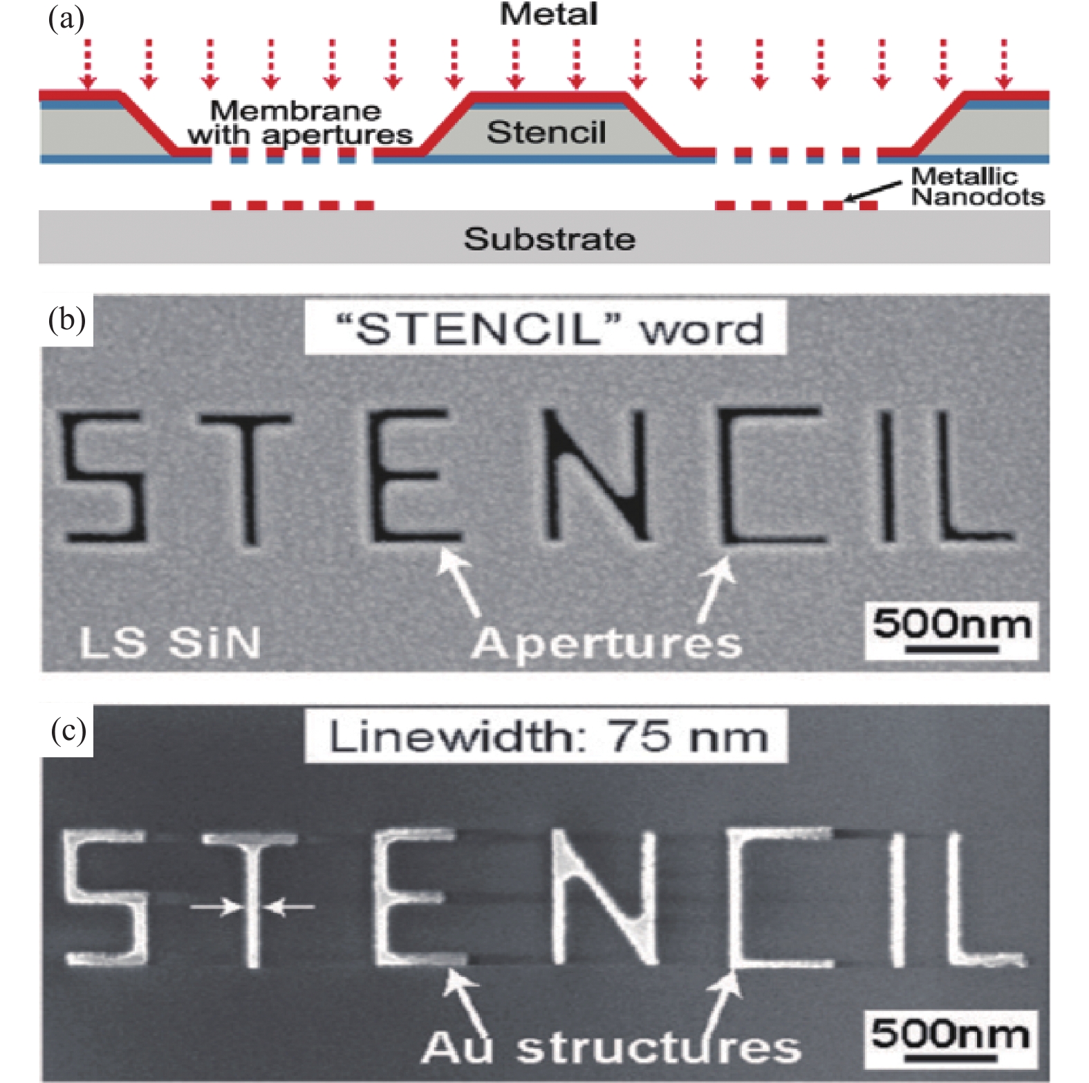
图 1 (a)一个具有镂空图案的掩模放置于衬底上的概略图。在蒸镀金属时,材料会通过镂空沉积在衬底上,重现掩模上的图案[70]。(b)一个具有纳米尺度镂空图案的氮化硅掩模,图案是一个“STENCIL”的字样[71]。(c)对应所沉积的、具有75纳米线宽的金图案,显示出从掩模到衬底的图案转移[71]。
Figure 1. (a) A schematic of a stencil mask containing apertures on top of a substrate. During the evaporation of a metal, the material passing through the apertures is deposited on the substrate, reproducing the pattern of the stencil mask[70]. (b) A silicon-nitride stencil mask with nanoapertures showing the word of “STENCIL”[71]. (c) The corresponding deposited structures of Au in 75-nm line width, showing the stencil-to-substrate pattern transfer[71].
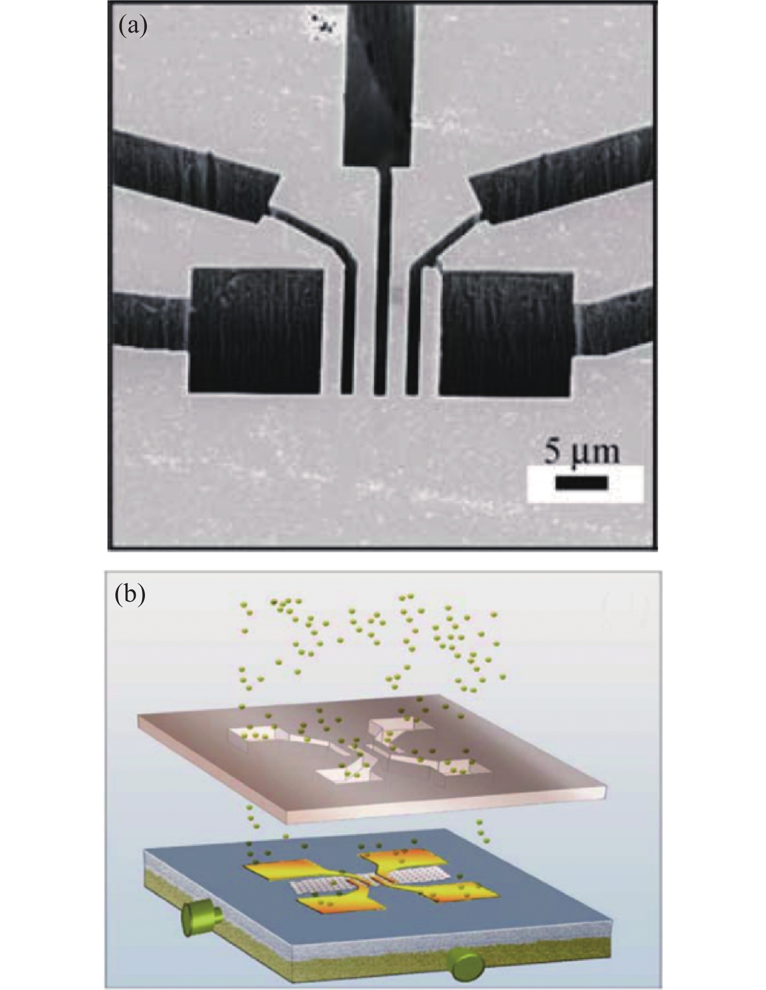
图 2 (a)一个制备的用于沉积金属接触的硅掩模的扫描电子显微镜图。(b)一个利用(a)的掩模沉积金属接触所得到的石墨烯器件概略图[83]
Figure 2. (a) A scanning electron microscopy image of the resulted silicon sencil mask for the deposition of metal contacts. (b) A schematic of graphene device fabricated by direct deposition of metal contacts throug the mask in (a) [83]
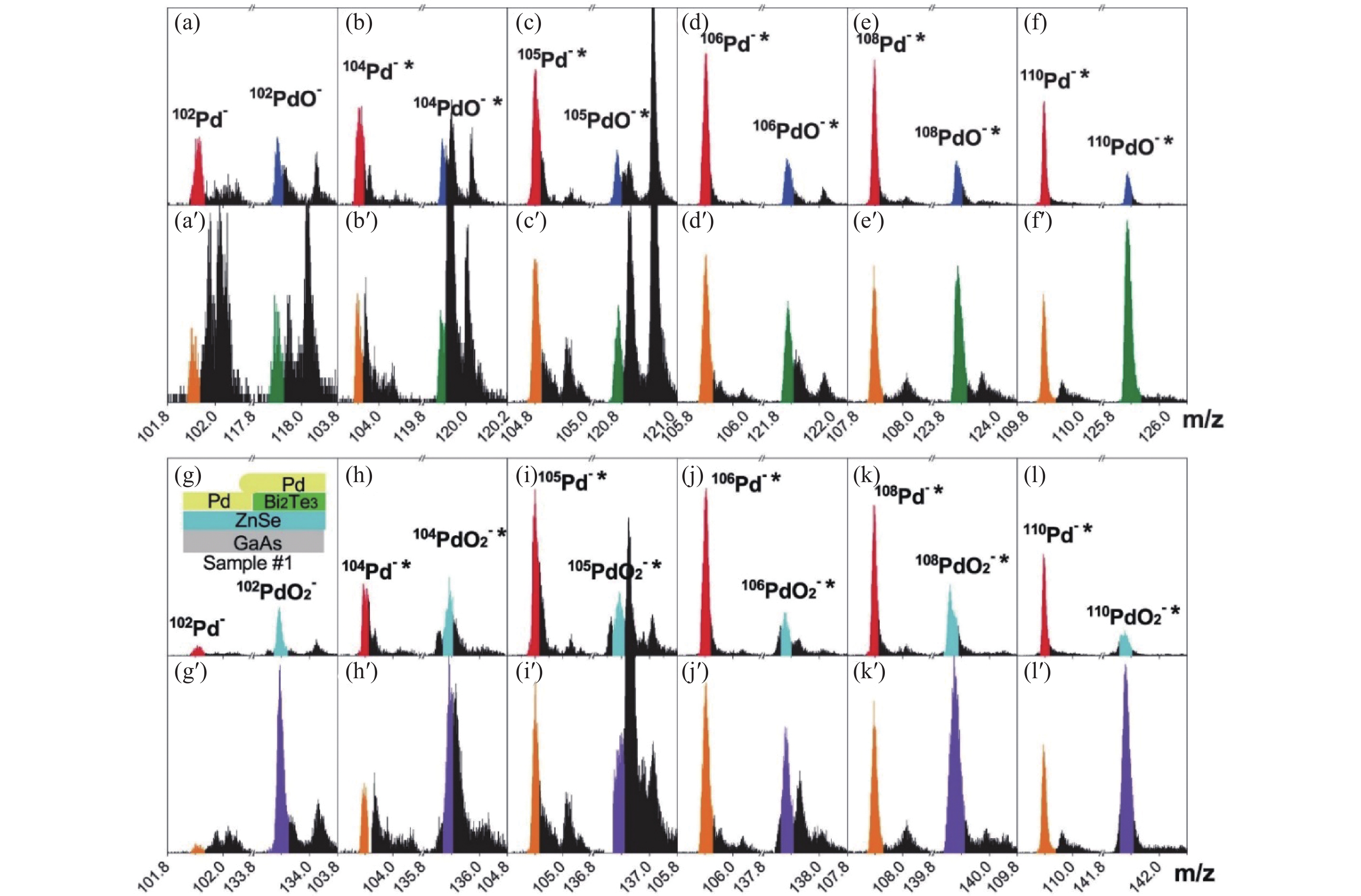
图 3 部分的时间飞行二次离子质谱。谱图采集于在干燥空气中暴露3天的有/没有Bi2Te3的区域,仅显示了Pd各个同位素质量Pd−, PdO− 和 PdO2−附近的数据。(a)-(f)和(g)-(l)显示从没有Bi2Te3的区域得到的数据,(a')-(f')和(g')-(l')显示从有Bi2Te3的区域得到的数据。插图显示了样品的结构[86]
Figure 3. Partial time-of-flight secondary ion mass spectra obtained from the regions without and with Bi2Te3 after exposing the sample in dry air for 3 days. Only the data in the neighborhoods of Pd−, PdO− and PdO2− for each of the isotopic masses of Pd are displayed. (a)–(f) and (g)–(l) show the data obtained from the region without Bi2Te3, while (a')–(f') and (g')–(l') are those obtained from the region with Bi2Te3. The inset of (g) displays the structure of the sample [86]
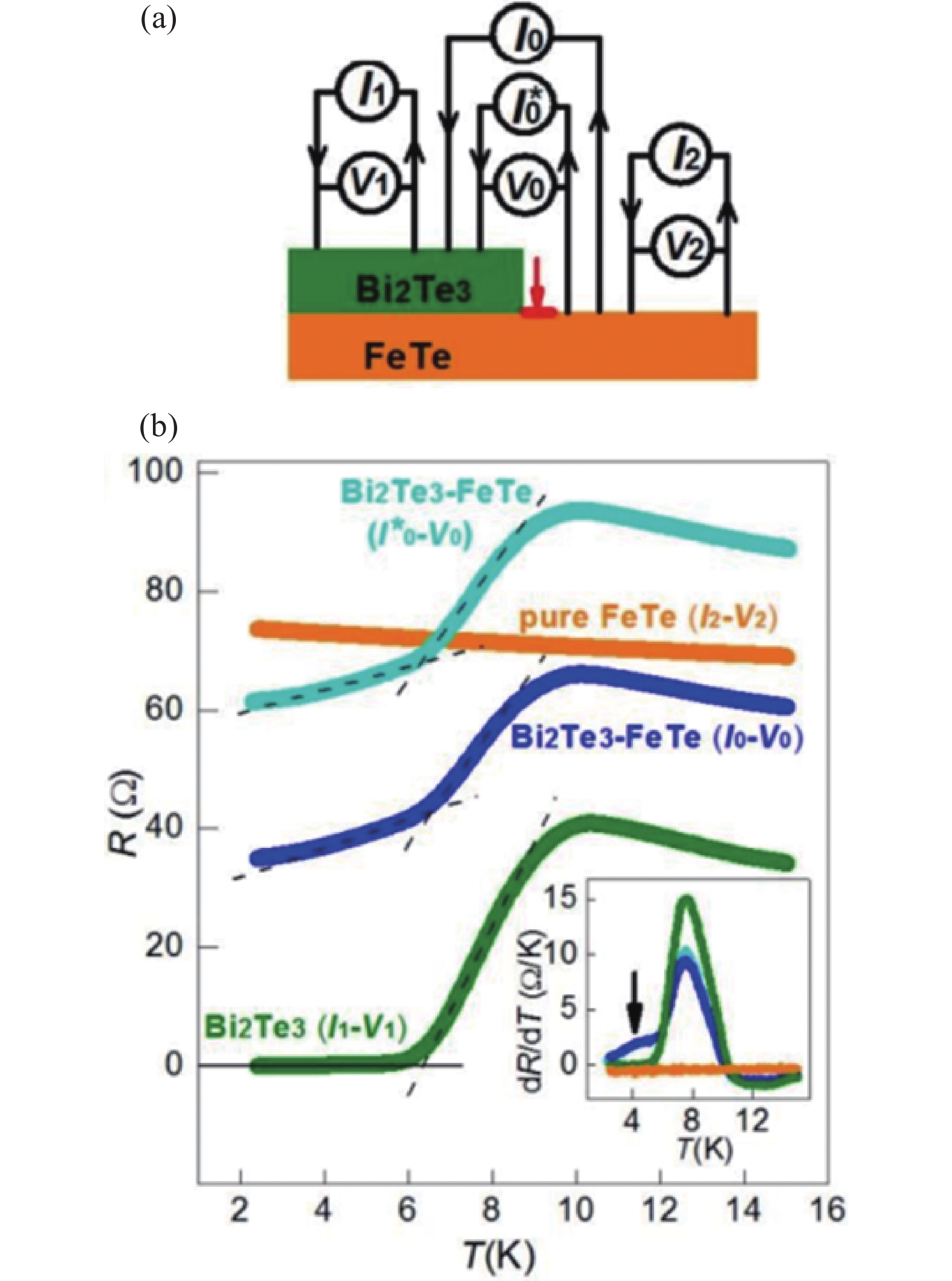
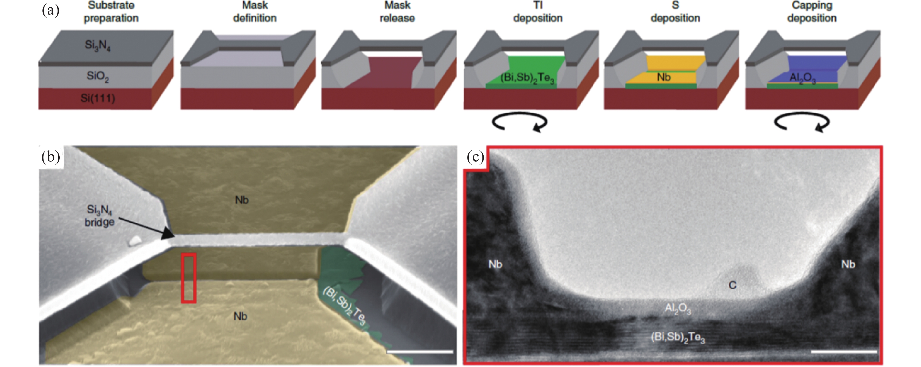
图 5 (a)利用掩模制备的拓扑绝缘体-超导体约瑟夫森结的过程。(b)所制备的结器件的扫描电子显微镜假彩色图。标尺长度:500 nm。(c)结器件横截面的透射电子显微镜图。标尺长度:20 nm [87]
Figure 5. (a) The fabrication processes of a topological insulator-superconductor Josephson junction using SL. (b) False colour scanning electron micrograph of the fabricated junction. Scale bar, 500 nm. (c) Transmission electron micrograph of the cross-section of the junction. Scale bar, 20 nm [87]
-
[1] Villanueva G,Vazquez-Mena O,van den Boogaart M A F,et al. Etching of sub-micrometer structures through Stencil[J]. Microelectronic Engineering,2008,85(5-6):1010−1014 doi: 10.1016/j.mee.2007.12.068 [2] Viallet B,Grisolia J,Ressier L,et al. Stencil-assisted reactive ion etching for micro and Nano patterning[J]. Microelectronic Engineering,2008,85(8):1705−1708 doi: 10.1016/j.mee.2008.04.027 [3] Dumas C,Grisolia J,Ressier L,et al. Synthesis of localized 2D-layers of silicon nanoparticles embedded in a SiO2 layer by a stencil-masked ultra-low energy ion implantation process[J]. Physica Status Solidi (A),2007,204(2):487−491 doi: 10.1002/pssa.200673232 [4] Villanueva L G,Martin-Olmos C,Vazquez-Mena O,et al. Localized Ion implantation through micro/nanostencil masks[J]. IEEE Transactions on Nanotechnology,2011,10(5):940−946 doi: 10.1109/TNANO.2010.2090171 [5] Chou S Y,Krauss P R,Renstrom P J. Imprint lithography with 25-nanometer resolution[J]. Science,1996,272(5258):85−87 doi: 10.1126/science.272.5258.85 [6] Villanueva L,Vazquez-Mena O,Martin-Olmos C,et al. Resistless fabrication of nanoimprint lithography (NIL) stamps using Nano-stencil lithography[J]. Micromachines,2013,4(4):370−377 doi: 10.3390/mi4040370 [7] Schallenberg T,Borzenko T,Schmidt G,et al. In situ size-control of CdZnSe Nano-islands using shadow masks[J]. Journal of Applied Physics,2004,95(1):311−315 doi: 10.1063/1.1631071 [8] Schallenberg T,Molenkamp L W,Karczewski G. Molecular beam epitaxy of compound materials through shadow masks[J]. Physical Review B,2004,70(15):155328 doi: 10.1103/PhysRevB.70.155328 [9] Köhler J,Albrecht M,Musil C R,et al. Direct growth of nanostructures by deposition through an Si3N4 shadow mask[J]. Physica E:Low-dimensional Systems and Nanostructures,1999,4(3):196−200 doi: 10.1016/S1386-9477(99)00007-7 [10] Shin H J,Choi J H,Yang H J,et al. Patterning of ferroelectric nanodot arrays using a silicon nitride shadow mask[J]. Applied Physics Letters,2005,87(11):113114 doi: 10.1063/1.2048818 [11] Salis G,Fuhrer A,Schlittler R R,et al. Temperature dependence of the nonlocal voltage in an Fe/GaAs electrical spin-injection device[J]. Physical Review B,2010,81(20):205323 doi: 10.1103/PhysRevB.81.205323 [12] Du K,Ding J J,Liu Y Y,et al. Stencil lithography for scalable micro- and nanomanufacturing[J]. Micromachines,2017,8(4):131 doi: 10.3390/mi8040131 [13] Vazquez-Mena O,Gross L,Xie S,et al. Resistless nanofabrication by stencil lithography: A review[J]. Microelectronic Engineering,2015,132:236−254 doi: 10.1016/j.mee.2014.08.003 [14] Allenspach R,Bischof A,Stampanoni M,et al. Growing thin magnetic films with a mask: Distinguishing between magnetic and instrumental asymmetries[J]. Applied Physics Letters,1992,60(15):1908−1910 doi: 10.1063/1.107150 [15] Schallenberg T,Schumacher C,Faschinger W. In situ structuring during MBE regrowth with shadow masks[J]. Physica E:Low-dimensional Systems and Nanostructures,2002,13(2-4):1212−1215 doi: 10.1016/S1386-9477(02)00338-7 [16] Speets E A,te Riele P,van den Boogaart M A F,et al. Formation of metal Nano- and micropatterns on self-assembled monolayers by pulsed laser deposition through nanostencils and electroless deposition[J]. Advanced Functional Materials,2006,16(10):1337−1342 doi: 10.1002/adfm.200500933 [17] Cojocaru C V,Harnagea C,Rosei F,et al. Complex oxide nanostructures by pulsed laser deposition through nanostencils[J]. Applied Physics Letters,2005,86(18):183107 doi: 10.1063/1.1923764 [18] Cojocaru C, Harnagea C, Pignolet A, et al. Patterning of functional materials by pulsed laser deposition through nanostencils[C]//2006 IEEE Conference on Emerging Technologies - Nanoelectronics, Singapore: IEEE, 2006: 283-288. [19] Langston M C,Usui T,Prinz F B. Mechanical masking of films deposited by atomic layer deposition[J]. Journal of Vacuum Science & Technology A:Vacuum, Surfaces, and Films,2012,30(1):01A153 [20] Zhang C,Kalliomäki J,Leskelä M,et al. Patterned films by atomic layer deposition using Parafilm as a mask[J]. Journal of Vacuum Science & Technology A:Vacuum, Surfaces, and Films,2018,36(1):01B102 [21] Astaneh S H,Sukotjo C,Takoudis C G,et al. Simple masking method for selective atomic layer deposition of thin films[J]. Journal of Vacuum Science & Technology B,2020,38(2):025001 [22] Ingle F W. A shadow mask for sputtered films[J]. Review of Scientific Instruments,1974,45(11):1460−1461 doi: 10.1063/1.1686529 [23] Barnabé A,Lalanne M,Presmanes L,et al. Structured ZnO-based contacts deposited by non-reactive rf magnetron sputtering on ultra-thin SiO2/Si through a stencil mask[J]. Thin Solid Films,2009,518(4):1044−1047 doi: 10.1016/j.tsf.2009.03.232 [24] Tokura Y,Kawasaki M,Nagaosa N. Emergent functions of quantum materials[J]. Nature Physics,2017,13(11):1056−1068 doi: 10.1038/nphys4274 [25] He Q L,Hughes T L,Armitage N P,et al. Topological spintronics and magnetoelectronics[J]. Nature Materials,2022,21(1):15−23 doi: 10.1038/s41563-021-01138-5 [26] Fu L,Kane C L,Mele E J. Topological insulators in three dimensions[J]. Physical Review Letters,2007,98(10):106803 doi: 10.1103/PhysRevLett.98.106803 [27] Zhang H J,Liu C X,Qi X L,et al. Topological insulators in Bi2Se3, Bi2Te3 and Sb2Te3 with a single Dirac cone on the surface[J]. Nature Physics,2009,5(6):438−442 doi: 10.1038/nphys1270 [28] Qi X L,Zhang S C. Topological insulators and superconductors[J]. Reviews of Modern Physics,2011,83(4):1057−1110 doi: 10.1103/RevModPhys.83.1057 [29] Hsieh D,Qian D,Wray L,et al. A topological Dirac insulator in a quantum spin Hall phase[J]. Nature,2008,452(7190):970−974 doi: 10.1038/nature06843 [30] Tokura Y,Yasuda K,Tsukazaki A. Magnetic topological insulators[J]. Nature Reviews Physics,2019,1(2):126−143 doi: 10.1038/s42254-018-0011-5 [31] Hasan M Z,Kane C L. Colloquium: Topological insulators[J]. Reviews of Modern Physics,2010,82(4):3045−3067 doi: 10.1103/RevModPhys.82.3045 [32] Yan B H,Felser C. Topological materials: Weyl semimetals[J]. Annual Review of Condensed Matter Physics,2017,8(1):337−354 doi: 10.1146/annurev-conmatphys-031016-025458 [33] Liu Z K,Zhou B,Zhang Y,et al. Discovery of a three-dimensional topological Dirac semimetal, Na3Bi[J]. Science,2014,343(6173):864−867 doi: 10.1126/science.1245085 [34] Lv B Q,Weng H M,Fu B B,et al. Experimental discovery of Weyl semimetal TaAs[J]. Physical Review X,2015,5(3):031013 doi: 10.1103/PhysRevX.5.031013 [35] Okamura Y,Minami S,Kato Y,et al. Giant magneto-optical responses in magnetic Weyl semimetal Co3Sn2S2[J]. Nature Communications,2020,11(1):4619 doi: 10.1038/s41467-020-18470-0 [36] Liu D F,Liang A J,Liu E K,et al. Magnetic Weyl semimetal phase in a Kagomé crystal[J]. Science,2019,365(6459):1282−1285 doi: 10.1126/science.aav2873 [37] Xu S Y,Liu C,Kushwaha S K,et al. Observation of Fermi arc surface states in a topological metal[J]. Science,2015,347(6219):294−298 doi: 10.1126/science.1256742 [38] He Q L,Pan L,Stern A L,et al. Chiral Majorana fermion modes in a quantum anomalous Hall insulator-superconductor structure[J]. Science,2017,357(6348):294−299 doi: 10.1126/science.aag2792 [39] Wiedenmann J,Bocquillon E,Deacon R S,et al. 4π-periodic Josephson supercurrent in HgTe-based topological Josephson junctions[J]. Nature Communications,2016,7:10303 doi: 10.1038/ncomms10303 [40] Liu C X,Sau J D,Stanescu T D,et al. Andreev bound states versus Majorana bound states in quantum dot-nanowire-superconductor hybrid structures: Trivial versus topological zero-bias conductance peaks[J]. Physical Review B,2017,96(7):075161 doi: 10.1103/PhysRevB.96.075161 [41] Wang M X,Liu C H,Xu J P,et al. The coexistence of superconductivity and topological order in the Bi2Se3 thin films[J]. Science,2012,336(6077):52−55 doi: 10.1126/science.1216466 [42] Gazibegovic S,Car D,Zhang H,et al. RETRACTED ARTICLE: Epitaxy of advanced nanowire quantum devices[J]. Nature,2017,548(7668):434−438 doi: 10.1038/nature23468 [43] Wang D F,Kong L Y,Fan P,et al. Evidence for Majorana bound states in an iron-based superconductor[J]. Science,2018,362(6412):333−335 doi: 10.1126/science.aao1797 [44] Xu J P,Wang M X,Liu Z L,et al. Experimental detection of a Majorana mode in the core of a magnetic vortex inside a topological insulator-superconductor Bi2Te3/NbSe2 heterostructure[J]. Physical Review Letters,2015,114(1):017001 doi: 10.1103/PhysRevLett.114.017001 [45] Rokhinson L P,Liu X Y,Furdyna J K. The fractional a. c. Josephson effect in a semiconductor–superconductor nanowire as a signature of Majorana particles[J]. Nature Physics,2012,8(11):795−799 doi: 10.1038/nphys2429 [46] Wang E Y,Ding H,Fedorov A V,et al. Fully gapped topological surface states in Bi2Se3 films induced by a d-wave high-temperature superconductor[J]. Nature Physics,2013,9(10):621−625 doi: 10.1038/nphys2744 [47] Sun H H,Zhang K W,Hu L H,et al. Majorana zero mode detected with spin selective Andreev reflection in the vortex of a topological superconductor[J]. Physical Review Letters,2016,116(25):257003 doi: 10.1103/PhysRevLett.116.257003 [48] Xu S Y,Alidoust N,Belopolski I,et al. Momentum-space imaging of Cooper pairing in a half-Dirac-gas topological superconductor[J]. Nature Physics,2014,10(12):943−950 doi: 10.1038/nphys3139 [49] Fu L,Kane C L. Superconducting proximity effect and Majorana fermions at the surface of a topological insulator[J]. Physical Review Letters,2008,100(9):096407 doi: 10.1103/PhysRevLett.100.096407 [50] Sato M,Ando Y. Topological superconductors: a review[J]. Reports on Progress in Physics,2017,80(7):076501 doi: 10.1088/1361-6633/aa6ac7 [51] Williams J R,Bestwick A J,Gallagher P,et al. Unconventional Josephson effect in hybrid superconductor-topological insulator devices[J]. Physical Review Letters,2012,109(5):056803 doi: 10.1103/PhysRevLett.109.056803 [52] Ashworth C. 2D materials: The thick and the thin[J]. Nature Reviews Materials,2018,3(4):18019 doi: 10.1038/natrevmats.2018.19 [53] Wilson N P,Yao W,Shan J,et al. Excitons and emergent quantum phenomena in stacked 2D semiconductors[J]. Nature,2021,599(7885):383−392 doi: 10.1038/s41586-021-03979-1 [54] Liu Y,Duan X D,Shin H J,et al. Promises and prospects of two-dimensional transistors[J]. Nature,2021,591(7848):43−53 doi: 10.1038/s41586-021-03339-z [55] Li X K,Collignon C,Xu L C,et al. Chiral domain walls of Mn3Sn and their memory[J]. Nature Communications,2019,10(1):3021 doi: 10.1038/s41467-019-10815-8 [56] Liu E K,Sun Y,Kumar N,et al. Giant anomalous Hall effect in a ferromagnetic Kagome-lattice semimetal[J]. Nature Physics,2018,14(11):1125−1131 doi: 10.1038/s41567-018-0234-5 [57] Kiyohara N,Tomita T,Nakatsuji S. Giant anomalous hall effect in the chiral antiferromagnet Mn3Ge[J]. Physical Review Applied,2016,5(6):064009 doi: 10.1103/PhysRevApplied.5.064009 [58] Nayak A K,Fischer J E,Sun Y,et al. Large anomalous Hall effect driven by a nonvanishing Berry curvature in the noncolinear antiferromagnet Mn3Ge[J]. Science Advances,2016,2(4):e1501870 doi: 10.1126/sciadv.1501870 [59] Muhlbauer S,Binz B,Jonietz F,et al. Skyrmion lattice in a chiral magnet[J]. Science,2009,323(5916):915−919 doi: 10.1126/science.1166767 [60] Reyren N,Thiel S,Caviglia A D,et al. Superconducting interfaces between insulating oxides[J]. Science,2007,317(5842):1196−1199 doi: 10.1126/science.1146006 [61] He Q L,Liu H C,He M Q,et al. Two-dimensional superconductivity at the interface of a Bi2Te3/FeTe heterostructure[J]. Nature Communications,2014,5:4247 doi: 10.1038/ncomms5247 [62] Kim N H,Jung J,Cho J,et al. Interfacial Dzyaloshinskii-Moriya interaction, surface anisotropy energy, and spin pumping at spin orbit coupled Ir/Co interface[J]. Applied Physics Letters,2016,108(14):142406 doi: 10.1063/1.4945685 [63] Yang H X,Thiaville A,Rohart S,et al. Anatomy of dzyaloshinskii-moriya interaction at Co/Pt interfaces[J]. Physical Review Letters,2015,115(26):267210 doi: 10.1103/PhysRevLett.115.267210 [64] He Q L,Yin G,Grutter A J,et al. Exchange-biasing topological charges by antiferromagnetism[J]. Nature Communications,2018,9(1):2767 doi: 10.1038/s41467-018-05166-9 [65] Pan L,Grutter A,Zhang P,et al. Observation of quantum anomalous hall effect and exchange interaction in topological insulator/antiferromagnet heterostructure[J]. Advanced Materials,2020,32(34):2001460 doi: 10.1002/adma.202001460 [66] He Q L,Kou X F,Grutter A J,et al. Tailoring exchange couplings in magnetic topological-insulator/antiferromagnet heterostructures[J]. Nature Materials,2017,16(1):94−100 doi: 10.1038/nmat4783 [67] Lee C,Katmis F,Jarillo-Herrero P,et al. Direct measurement of proximity-induced magnetism at the interface between a topological insulator and a ferromagnet[J]. Nature Communications,2016,7:12014 doi: 10.1038/ncomms12014 [68] Katmis F,Lauter V,Nogueira F S,et al. A high-temperature ferromagnetic topological insulating phase by proximity coupling[J]. Nature,2016,533(7604):513−516 doi: 10.1038/nature17635 [69] Yang W M,Yang S,Zhang Q H,et al. Proximity effect between a topological insulator and a magnetic insulator with large perpendicular anisotropy[J]. Applied Physics Letters,2014,105(9):092411 doi: 10.1063/1.4895073 [70] Vazquez-Mena O,Sannomiya T,Villanueva L G,et al. Metallic nanodot arrays by stencil lithography for plasmonic biosensing applications[J]. ACS Nano,2011,5(2):844−853 doi: 10.1021/nn1019253 [71] Vazquez-Mena O,Sannomiya T,Tosun M,et al. High-resolution resistless nanopatterning on polymer and flexible substrates for plasmonic biosensing using stencil masks[J]. ACS Nano,2012,6(6):5474−5481 doi: 10.1021/nn301358n [72] Hyun W J,Secor E B,Hersam M C,et al. High-resolution patterning of graphene by screen printing with a silicon stencil for highly flexible printed electronics[J]. Advanced Materials,2015,27(1):109−115 doi: 10.1002/adma.201404133 [73] Azimi S,Song J,Li C J,et al. Nanoscale lithography of LaAlO3/SrTiO3 wires using silicon stencil masks[J]. Nanotechnology,2014,25(44):445301 doi: 10.1088/0957-4484/25/44/445301 [74] Deshmukh M M,Ralph D C,Thomas M,et al. Nanofabrication using a stencil mask[J]. Applied Physics Letters,1999,75(11):1631−1633 doi: 10.1063/1.124777 [75] Deng T,Li M W,Chen J,et al. Controllable fabrication of pyramidal silicon nanopore arrays and nanoslits for nanostencil lithography[J]. The Journal of Physical Chemistry C,2014,118(31):18110−18115 doi: 10.1021/jp503203b [76] Blech V,Nobuyuki T,Kim B. Nanostenciling through a cm2-wide silicon membrane[J]. Journal of Vacuum Science & Technology B:Microelectronics and Nanometer Structures Processing, Measurement, and Phenomena,2006,24(1):55−58 [77] Kölbel M,Tjerkstra R W,Kim G,et al. Self-assembled monolayer coatings on nanostencils for the reduction of materials adhesion[J]. Advanced Functional Materials,2003,13(3):219−224 doi: 10.1002/adfm.200390033 [78] Kölbel M,Tjerkstra R W,Brugger J,et al. Shadow-mask evaporation through monolayer-modified nanostencils[J]. Nano Letters,2002,2(12):1339−1343 doi: 10.1021/nl025784o [79] Savu V,Kivioja J,Ahopelto J,et al. Quick and clean: stencil lithography for wafer-scale fabrication of superconducting tunnel junctions[J]. IEEE Transactions on Applied Superconductivity,2009,19(3):242−244 doi: 10.1109/TASC.2009.2019075 [80] Allain A,Kang J H,Banerjee K,et al. Electrical contacts to two-dimensional semiconductors[J]. Nature Materials,2015,14(12):1195−1205 doi: 10.1038/nmat4452 [81] Kwon S Y. Integrating 2D materials and metal electrodes[J]. Nature Electronics,2022,5(5):259−260 doi: 10.1038/s41928-022-00770-6 [82] Jain A,Bharadwaj P,Heeg S,et al. Minimizing residues and strain in 2D materials transferred from PDMS[J]. Nanotechnology,2018,29(26):265203 doi: 10.1088/1361-6528/aabd90 [83] Staley N,Wang H,Puls C,et al. Lithography-free fabrication of graphene devices[J]. Applied Physics Letters,2007,90(14):143518 doi: 10.1063/1.2719607 [84] Bao W Z,Liu G,Zhao Z,et al. Lithography-free fabrication of high quality substrate-supported and freestanding graphene devices[J]. Nano Research,2010,3(2):98−102 doi: 10.1007/s12274-010-1013-5 [85] Chen H,Zhu W G,Xiao D,et al. CO oxidation facilitated by robust surface states on Au-covered topological insulators[J]. Physical Review Letters,2011,107(5):056804 doi: 10.1103/PhysRevLett.107.056804 [86] He Q L,Lai Y H,Lu Y,et al. Surface reactivity enhancement on a Pd/Bi2Te3 heterostructure through robust topological surface states[J]. Scientific Reports,2013,3:2497 doi: 10.1038/srep02497 [87] Schüffelgen P,Rosenbach D,Li C,et al. Selective area growth and stencil lithography for in situ fabricated quantum devices[J]. Nature Nanotechnology,2019,14(9):825−831 [88] Schmitt T W,Connolly M R,Schleenvoigt M,et al. Integration of topological insulator Josephson junctions in superconducting qubit circuits[J]. Nano Letters,2022,22(7):2595−2602 doi: 10.1021/acs.nanolett.1c04055 [89] Ohkouchi S,Nakamura Y,Ikeda N,et al. In situ mask designed for selective growth of InAs quantum dots in narrow regions developed for molecular beam epitaxy system[J]. Review of Scientific Instruments,2007,78(7):073908 doi: 10.1063/1.2756624 [90] Tun T N,Lwin M H T,Kim H H,et al. Wetting studies on Au nanowires deposited through nanostencil masks[J]. Nanotechnology,2007,18(33):335301 doi: 10.1088/0957-4484/18/33/335301 [91] Vazquez-Mena O,Villanueva L G,Savu V,et al. Analysis of the blurring in stencil lithography[J]. Nanotechnology,2009,20(41):415303 doi: 10.1088/0957-4484/20/41/415303 [92] Lishchynska M,Bourenkov V,van den Boogaart M A F,et al. Predicting mask distortion, clogging and pattern transfer for stencil lithography[J]. Microelectronic Engineering,2007,84(1):42−53 doi: 10.1016/j.mee.2006.08.003 [93] Rácz Z,Seabaugh A. Characterization and control of unconfined lateral diffusion under stencil masks[J]. Journal of Vacuum Science & Technology B:Microelectronics and Nanometer Structures Processing, Measurement, and Phenomena,2007,25(3):857−861 [94] Tiggelaar R M,Berenschot J W,Elwenspoek M C,et al. Spreading of thin-film metal patterns deposited on nonplanar surfaces using a shadow mask micromachined in Si (110)[J]. Journal of Vacuum Science & Technology B:Microelectronics and Nanometer Structures Processing, Measurement, and Phenomena,2007,25(4):1207−1216 -
计量
- 文章访问数: 274
- HTML全文浏览数: 274
- PDF下载数: 3
- 施引文献: 0