
 首页
首页 登录
登录 注册
注册


 下载:
下载:
-
20世纪60年代初,美国斯坦福研究所(SRI)的Shoulders 首次提出发展开关速度在10−10 s的微米级的真空隧道效应器件的概念,并开始真空集成电路的研究[1]。1968年,同在SRI的Spindt博士成功地利用电子束加工技术和薄膜技术加工出了金属钼薄膜场致发射阵列阴极,又称Spindt阴极[2],并在1976年报道了大面积阵列的制造技术及其物理特性,得到广泛认可[3],从此开启了真空微电子学研究的时代。
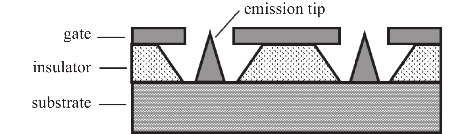
Spindt阴极是硅片上由成千上万个发射单元组成的阵列,每个发射单元由基极、钼发射体尖锥、二氧化硅绝缘层和自对准钼栅极组成,结构如图1所示。由于发射体锥尖曲率半径一般只有几十纳米,发射体锥尖与栅极间距近,栅极相对锥尖加很低的正偏压时,锥尖表面就会产生强电场,使其表面势垒高度降低宽度变窄,电子通过隧道效应逸出,且改变栅极电压可以调控发射电流大小。在阴极制作过程中,还可以通过控制工艺条件,使得封装密度高达每平方厘米几千万个的发射单元中各尖锥具有基本相同的场增强因子,大量集成发射体尖锥的共同发射,使得整个阴极具有很大的电流密度和总电流。基于先进的微纳加工技术制备的Spindt阴极相较于传统热电子源有许多优势,可以瞬时启动、工作电压低、可在常温下工作,以及由于其制备方式与半导体工艺兼容,发射体形状、位置、集成度可控性强,因此Spindt阴极被认为是适合用于真空电子器件的冷阴极电子源。
自此,研究者们对Spindt阴极进行了广泛而深入的研究,以不断完善和提升其性能,并取得了不错的研究成果。到目前为止,Spindt阴极仍保持多项最优记录:如单尖发射电流可达1 mA,最大电流密度达2000 A/cm2,实验室寿命达8年[4]。
由于Spindt阴极的微细结构制作工艺复杂,加工难度很大,且难以实现大面积制作。近几十年来,研究者们致力于从结构、材料以及工艺技术方面提高Spindt阴极的场发射特性以及耐用性,力求在低电压均匀稳定发射高电流密度的同时,提高抵御离子轰击、电弧伤害等能力。本文针对Spindt阴极的研究新进展以及面临的问题进行综述。
-
典型的Spindt阴极制作工艺流程如图2所示。首先利用热氧化技术和磁控溅射技术在硅片上形成二氧化硅绝缘层和钼栅极层;采用光学光刻以及电感耦合反应离子刻蚀技术得到栅极孔,通过湿法腐蚀二氧化硅孔得到带自对准栅极孔的空腔,在真空镀膜系统中,通过掠射角沉积氧化铝牺牲层和垂直方向沉积钼的双向沉积技术,得到场发射金属钼尖锥,最后,剥离牺牲层,连带去除牺牲层上的多余钼层,完成Spindt阴极的制作。
-
原始的Spindt型场发射阵列形成需要铝牺牲层的掠角沉积和发射极尖锥形成的定向沉积,这些沉积通常使用电子束蒸发设备实现,因此,当使用大型基板(例如用于显示应用的米级基板)时,制造设备会变得更大,难以实现大面积制造。Nagao M等介绍了一种新的Spindt型场发射器的制备方法,使用双层光刻胶作为牺牲层,并使用高功率脉冲磁控溅射代替电子束蒸发工艺来形成发射体尖锥。采用蚀刻技术[5],在每个发射锥上形成多栅极聚焦电极,该工艺将使得在大型基板上形成Spindt发射器成为可能[6]。
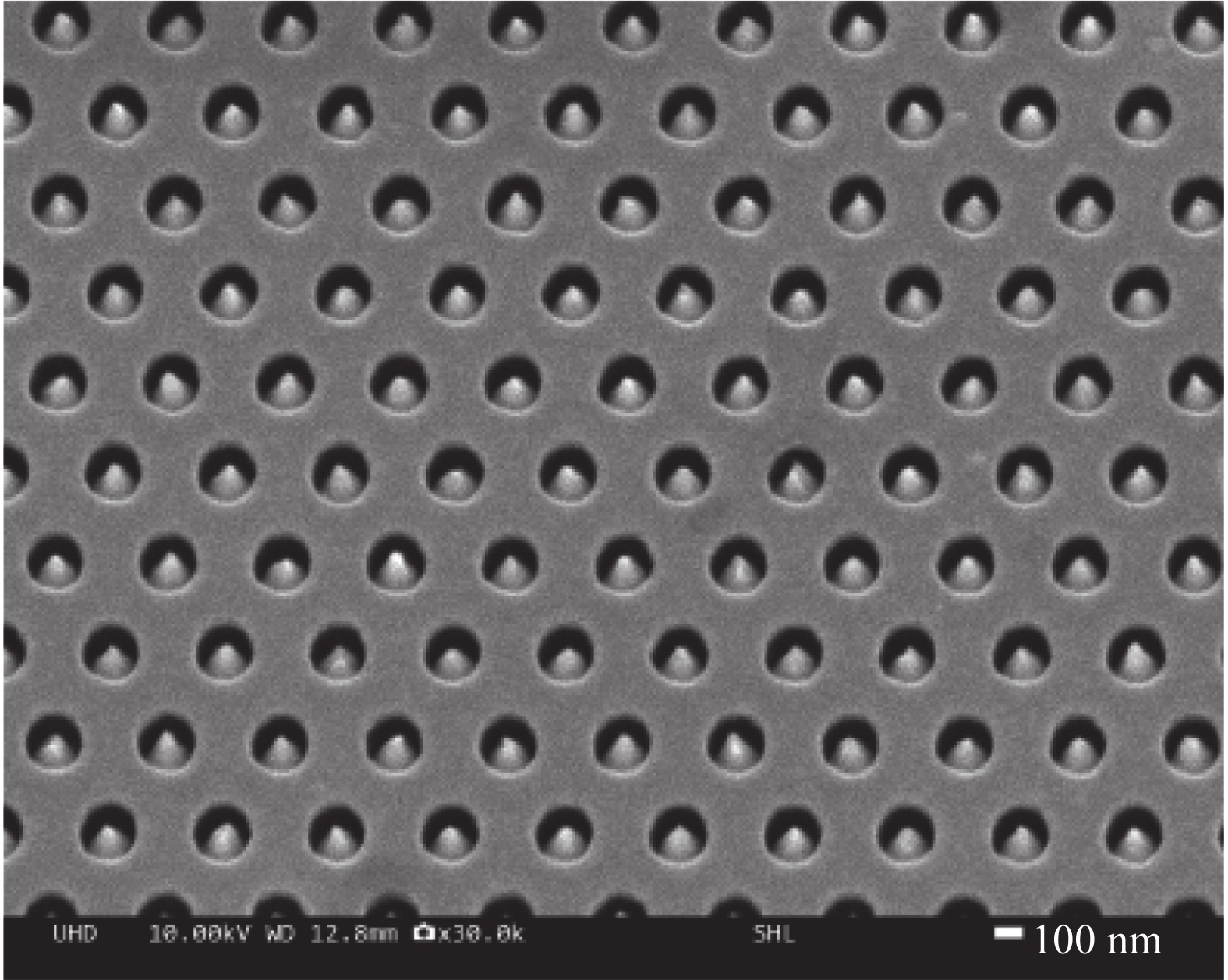
Spindt阴极的工作电压一般在100 V左右,在实际应用中,希望工作电压越低越好。通过改进的纳米球光刻法(图3)来改变栅极孔径的几何形状进而能够制备出更尖锐的钼发射尖(图4)[7],与未采用这种方法加工的发射尖相比,开启电压从120 V降低到了35 V。该制备方法促进了高密度栅控场发射器件的低成本和大面积的应用[8]。
Spindt阴极的场发射性能与尖锥表面形貌息息相关,强电场作用、离子的轰击以及局部的升温都会引起尖锥形貌的变化,尖锥表面气体分子的吸附和脱附也会改变其功函数,甚至会导致不期望的电弧产生[9]。为避免发生空间电弧,损伤阴极及器件,要对阴极进行很充分的后处理过程,例如真空烘烤以及等离子体清洗技术可以消除阴极表面污染和吸附[10],阴极老练以及表面涂覆可以改善发射面表面状态,使其能稳定高效地工作[11-12]。
研究发现H2与活性钼场发射阵列的相互作用可以作为一种高效、超高真空兼容的场发射阵列原位清洁方法。引入系统的H2气体发生离解和电离,氢原子和氢离子与钼相互作用,形成挥发性的钼氢化物,挥发性物质通过真空系统去除。一定量的氢气处理会使发射器表面功函数降低从而使发射增强[13]。SRI报道了一种基于发射体尖锥在工作过程中自加热的原位处理方法,证明了该方法可以通过平整和清洁发射体尖锥从而提高尖锥之间的发射均匀性。将该方法应用于50000个尖锥阵列时,其产生了300 mA的发射电流(发射电流密度为40 A/cm2),预计通过对实验装置进行适当的改进,可以得到1 A的发射电流(发射电流密度为100 A/cm2)。改进的均匀性允许在高电流、高电流密度工作器件提高阴极可靠性[14]。此外,研究发现在使用紫外线照射1000×1000个尖端栅控场发射阵列60 min后,栅极电流降低了10倍以上,而发射电流提高了10倍以上。这表明紫外线可以通过清洁场发射阵列,即发射极表面以及栅极和发射极之间的电介质的解吸(主要是水和其它物质)来影响场发射阵列的性能[15],该方法在Spindt型GaN阵列中也得到了验证[16]。
-
除了根据Spindt型冷阴极结构进行工艺优化来达到提升阴极性能的目的,随着先进微电子技术的发展,研究者们设计了多种以Spindt型冷阴极为基础的变型结构,使其在性能提升和应用方面得到了广泛的发展。
场发射阵列通常存在光束发散问题,即电子是从具有提取栅极的场发射阵列以20°或者更大半角的锥形方向发射,而在实际应用中,将电子束准直成一个小光斑是至关重要的。在火山结构双栅场发射阵列中(图5)[17-19],下栅极(提取电极)从尖端提取电子束,上栅极(聚焦电极)施加比提取电极电压更低的电压,用来作为静电聚焦透镜控制电子轨迹。相较于早期传统的双栅结构场发射阵列[20],可以在不会极大减少发射电流的情况下聚焦电子束,实现高聚焦电子束和高发射电流。
利用火山型阵列的外层集成电极作为偏负压离子收集器来削弱离子反轰击,从而提高了阴极的电流稳定性和可靠性,这项工作为提高低真空运行冷阴极的寿命提供了一种思路[21]。火山结构双栅场发射阵列可以以矩阵模式驱动,在具有超高灵敏度、高辐射耐受性的图像传感器应用方向前景广阔[22-23]。针对火山结构开发了最小制造系统结合传统半导体制造设备的混合工艺制造火山结构Spindt型场发射阵列,减少了投资,适用于低批量生产产品,对于开发真空纳米电子器件将有重要意义[24]。
倒模成型技术可制备出顶点尺寸均匀可控的全金属场发射阵列[25]。全金属发射阵列是在金属基底上制备出金字塔型钼场发射阵列,该结构具有更高的热导率和热传播,有利于尖端在高发射电流下的热稳定性。新的工艺方法可以在纳米尺度控制发射尖端顶点曲率,可以抵抗尖端的电迁移和熔化,从而提高单尖端电流。使用聚焦离子束辅助法在倒模成型技术的基础上制造准直栅电极比自对准回蚀方法更可靠和稳定[26]。在上述研究基础上,提出了一种制造大规模和高密度全金属栅控纳米发射器的方法(图6),所制备的高密度发射体纳米尖端顶点的局域电场与微米级发射体一样高。这些阵列具有片上电子提取栅电极和多达106个金属纳米尖锥,尖锥密度超过108 cm−2。其器件结构适用于高频电开关,对于需要微型高亮度电子源的应用很有前途。这些阵列有希望通过实现具有超快激光脉冲的亚微米间距场发射阵列的触发,从而找到作为超快阴极的应用[27]。
通过氟基电感耦合等离子体 (ICP) 蚀刻直接在钼衬底中制造高纵横比(>10)场发射全金属尖锥(图7),与传统的Spindt 阵列相比,该器件消除了薄膜界面,并且该器件表现出1.21 V/μm的低导通电场。采用1,000,000个针尖阵列,间距为10 μm,在5.48 V/μm的电场强度下发射140 μA的电流。在场发射显示中观察到稳定、均匀的发射。Mo-FEA具有更好的导电性和导热性,在长期和连续发射方面非常有前途,特别是在需要高电流密度的高质量小型化行波管(TWT)领域[28]。
-
尽管Spindt阴极性能优越,但很难实现真正的实用化,归根结底在于Spindt阴极的低可靠性,例如器件短路造成的成品率不高、发射单元的非均匀发射导致的局部过热损毁,以及空间电弧损伤所导致的阴极失效等。
-
近年来对Spindt阴极的研究工作主要集中在通过优化关键工艺提升阴极品质,以及探究阴极失效机理,提高可靠性方面[29-30]。
阴栅短路失效问题一直都是限制Spindt阴极发展的瓶颈问题,严重影响着阴极成品率,但国内外对短路失效问题的研究和报道少之又少。作者所在的实验室研究发现金属颗粒粘附是导致短路失效的主要原因[31],通过对其进行机理分析、工艺研究、结构优化、后处理等,重点为解决Spindt阴极阴栅短路失效问题提出合理的方案[32]。Spindt阴极绝缘层空腔由湿法腐蚀制得,该工艺得到的空腔为碗型(图8(a),直径约4 µm),有极大的空间容纳工艺过程中残留的金属颗粒,将工艺优化为干法刻蚀与湿法腐蚀相结合的方法,可得到圆柱型绝缘层空腔(图8(b),直径约1.3 µm),有利于残留金属颗粒从栅极孔(直径约1 µm)中洗出,结果表明该工艺和结构的优化有利于金属颗粒在后续清洗工艺中从空腔中洗出,极大地减少了金属颗粒的残留,样品的成品率(阴栅不短路)提高到了约50%。
-
一直以来,传统观点认为,当在高发射水平下工作时,阵列中发射极尖端之间的一致性差会导致部分发射极尖端产生过度发射、过热和熔毁,从而产生使结构短路的电弧[33]。在开发基于Spindt阴极的中子发生器场解吸离子源的过程中,为了改善高电压造成的电击穿以及结构损坏的问题,优化了传统的Spindt阴极结构,采用Si3N4绝缘屏蔽层抑制栅极的电子发射(图9)[34]。该研究确定了在高发射水平下造成破坏阴极电弧的原因不是发射极尖端爆炸熔毁,而是由于阴极腔底部由硅、二氧化硅和真空形成的三相点的伪发射,触发了电子沿氧化物侧壁的闪络,对阴极阵列产生破坏[35]。该结构表现出良好的可靠性,为开发用于行波管的发射极阵列,SRI设计了1 mm直径阵列内包含有14000发射尖锥的发射极,在25 Hz脉冲和100 mA连续波下,成功在175 mA电流下工作100 h[36]。带屏蔽栅的Spindt型场发射源与高迁移率GaN光电导半导体开关集成在一起,开发了能够在皮秒脉冲状态下产生安培级电流的阴极[37]。
事实上,在该结构制备过程中,几个微米直径量级的屏蔽层孔与栅极孔套刻工艺实现难度极大,对设备要求非常高。作者所在的实验室以降低高压下三叉点电弧放电失效为出发点,设计并制作了多绝缘层Spindt阴极结构(图10-11),即在典型Spindt阴极单一SiO2绝缘层中加入Si3N4,从而形成侧壁崎岖的结构,可阻止电子的沿面闪络放电。该结构制备方法不需要套刻工艺,降低了制作成本,具有十分重要的意义[38]。
-
Spindt型阴极在微波真空器件中的应用是冷阴极的重要研究方向之一。冷阴极具有瞬时启动、工作电压低、可在常温下工作等优点,因此成为目前几乎专门用于微波真空器件的热离子发射器的有吸引力的替代品。Spindt型阴极阵列电流密度和总阵列电流已满足或超过许多中等功率行波管电子束要求的值,将Spindt型冷阴极用于行波管的研究在近20年来从未中断过。
Spindt栅控阴极实现了在C波段频率范围内高达30%的调制[39]。基于带屏蔽层的Spindt阴极,在X/Ku波段频率范围内测试TWT工作所需的电流和电流密度,在100 mA电流下,连续波运行时间达到创纪录的100 h[40]。冷阴极行波管开发和场发射阴极开发使TWT稳步延长寿命(图12),迄今为止任何冷阴极TWT报告的最长运行寿命超过1000小时[41]。研究者们期望开发一种具有相当发射性能的阴极,能够驱动TWT在>90 GHz的毫米波频率工作。在100 GHz频率下工作的TWT需要小于标准场发射极阵列的~2 mm-mrads的发射率。标准发射极阵列相对于热离子阴极的更高发射率最终导致需要接近6000 G的周期性永磁(PPM)场峰值。由于现有的稀土磁体无法实现这一磁场,通过为每个发射器尖端引入静电聚焦电极来实现发射率降低(图13),构建低发射率(< 0.5 mm-mrad)的Spindt 阴极[42]。
当微波真空管工作频率上升到太赫兹频段,高频互作用系统尺寸急剧减小,具有小面积、强发射性能特征的冷阴极更具优势,但目前国际上主要以碳纳米管阴极等作为电子源[43-44],国内也几乎没有出现Spindt阴极太赫兹真空器件的报导[45]。
-
除了如前所述的行波管,一些机构的项目也尝试在回旋加速器[46]、速调管[47]中进行Spindt型冷阴极研究。与此同时,研究人员也一直在探索Spindt型场发射器技术在X射线产生方面的潜力。
断层合成(TS)成像的线性X射线源原型有50000个发射尖锥的阴极发射实现高达50 kV的X射线,每个发射器单元使用直径为750 nm的栅极孔径。发射始于高于60 V的栅极偏置[48]。在这项工作的基础上,开发了一种使用更精细光刻技术的更先进的场发射阴极[49]。该阴极在硅晶圆上制造,通过使用直径为200 nm的栅极孔径能够将超过5000万个发射器尖锥集成到一个直径为3 mm的圆中(图14)。将Spindt场发射阴极应用于X射线管中,可以在30−160 kV的宽阳极偏压范围内高效运行,当阳极偏置为120 kV时,X射线管功率高于1 kW,这足以用于医疗X射线成像,栅极偏置低于35 V。冷阴极表现出的电流−电压特性在很大程度上不受阳极偏置的影响。该管的多能量X射线彩色扫描功能除了具有执行静止CT扫描的原生能力外,还具有材料识别的额外优势(图15)。
-
Spindt型火山结构双栅场发射阵列出现之后,研究者将这种新型静电聚焦Spindt型场发射器阵列(FEA)和高增益雪崩冲击非晶光电导体(HARP)目标组成平面图像传感器,称为FEA-HARP图像传感器,改善了发射电子束的扩散,目的是开发超高灵敏度紧凑型HDTV摄像机[50-52],该研究使Spindt阴极再次在显示领域得到应用。2023年,使用具有Ni尖端的Spindt型火山结构双栅场发射阵列的原型HARP-FEA图像传感器拍摄并显示示了具有均匀图像强度的再现图像,表明了在没有磁聚焦的情况下产生了静电聚焦效应。所开发的这种摄像机可用于广播、医学、自然科学和安全等各个领域[17, 53-54]。
-
Spindt阴极无论是在微波真空电子器件,还是X射线管等领域都尚未实现真正的应用,原因是在应用研究过程中,更多的是关注其大电流以及大电流密度的优势,而在此工作状态下,阴极极易发生损毁,达不到预期寿命。针对目前应用现状,除了不断提高Spindt阴极的性能以满足在高功率高频率领域的需求,探索小电流工作环境的应用,发挥其常温工作、功耗低等优势或许可以带来更高的可靠性,实现其应用价值,助力更多真空器件小型化。
精确计时对导航、通信和科学研究至关重要。广受欢迎的全球定位系统(GPS)之所以成为可能,要归功于其卫星上的原子钟。虽然GPS已成为现代导航系统的支柱,但GPS信号容易受到干扰。在这种GPS被干扰的环境中,用户端的小原子钟可以在本地提供稳定的频率参考,以支持其导航系统并减少中断的影响。在过去的几十年里,人们付出了相当大的努力来减小原子钟的尺寸和功率,并利用不同的方法提高原子钟的鲁棒性。捕获的原子或离子可以消除壁碰撞效应,从而实现更高的稳定性和准确性,因此,捕获离子对微型原子钟具有吸引力。
2021年,Spindt型场发射极阵列作为低功率电离电子源,成为实现微汞离子钟尺寸和功耗最小化的一个关键组件[55]。汞离子是通过电子轰击产生的。带有欧姆灯丝加热器的阴极历来被用作电子源,其消耗高达几瓦。在微汞离子钟中,直接集成到真空阱管中的场发射极阵列(图16(d)),无需加热器,降低功耗,需要大约 100 V DC从场发射极尖端提取足够的电子电流。只需几微安电流,即可在几分钟内将大约几百万的汞离子完全加载到阱中,并使离子能够连续加载以实现不间断的时钟操作。Spindt阴极的使用还消除了阴极心脏在潜伏期间的放气,进一步提高了稳定性。在微型无泵真空四极阱管中开发的微汞离子钟原型,实现了一天内达到10−14的稳定水平,整个系统的SWaP(尺寸、重量和功率)为1.1 L、1.2 kg和<6 W功率,原型钟已经运行了30多个月[56]。该工作为Spindt阴极在小电流工作的新领域的应用提供了思路。
-
Spindt阴极相较于传统热阴极有许多优势,例如可以瞬时启动、工作电压低、可在常温下工作,制备方式与半导体工艺兼容等,在真空电子器件领域有广泛的应用前景。以Spindt阴极作为电子源的真空电子器件,不仅可以实现耐高温、高速度、高频率和大功率,也可以同时具有小体积、高效率、和低成本。为了进一步推动Spindt阴极实用化进程,国内外研究者基于先进的微纳加工技术优化关键制造工艺以及创新多种变型结构提高Spindt阴极的场发射特性以及可靠性,力求在低电压均匀稳定发射高电流密度的同时,提高抵御离子轰击、电弧伤害等能力。
Spindt阴极未来的发展需要研究者们解放思想,继续探索新的工艺思路以更好地优化解决成品率低、可靠性差的瓶颈问题。与此同时,也要脚踏实地扎根在基础研究,继续完善Spindt阴极理论体系。在应用方面,除了不断提高Spindt阴极的性能以满足高功率和高频率真空电子器件的需求,也要拓宽思维寻找和探索其它应用新领域,Spindt阴极作为低功率电离电子源在微汞离子钟中的应用吸引了研究者们的注意,小电流、低能量、高可靠性的工作环境或成为Spindt阴极新的应用方向,使其在更多真空电子器件中发挥作用。
Spindt阴极研究进展和面临的问题
Research Progress and Facing Challenges of Spindt Cathode
-
摘要: 基于先进的微纳加工技术制备的Spindt阴极相比于热阴极具有可以瞬时启动、工作电压低、可在常温下工作等优势。尽管Spindt阴极性能优越,但很难实现真正的实用化,归根结底在于Spindt阴极的低可靠性。近几十年来,国内外研究者致力于从结构、材料以及工艺技术方面提高Spindt阴极的场发射特性以及耐用性,除了不断提高Spindt阴极的性能以满足高功率和高频率真空电子器件的需求,也在寻找和探索其它小电流、低能量、高可靠性的应用新领域,以更好地发挥Spindt阴极的优势。文章对Spindt阴极的最新研究进展进行了综述。Abstract: The Spindt cathode based on advanced micro/nano processing technology has many advantages over the present thermionic cathode, for example, instant start, low working voltage, and the ability to work at room temperature, etc. Despite the superior performance of the Spindt cathode, it is difficult to achieve practicality, ultimately due to the low reliability of the Spindt cathode. In recent decades, researchers have committed to improving the field emission performance and reliability of Spindt cathode in terms of structure, materials, and process technology. In addition to continuously improving the performance of Spindt cathode to meet the needs of high frequency and high power vacuum electronic devices, researchers are also seeking and exploring other new fields with low current, low energy, and high reliability to better leverage the advantages of Spindt cathodes. The article provides a review of the latest research progress on Spindt cathodes.
-
Key words:
- Spindt cathode /
- Micro/nano processing technology /
- Vacuum electronic devices .
-

-
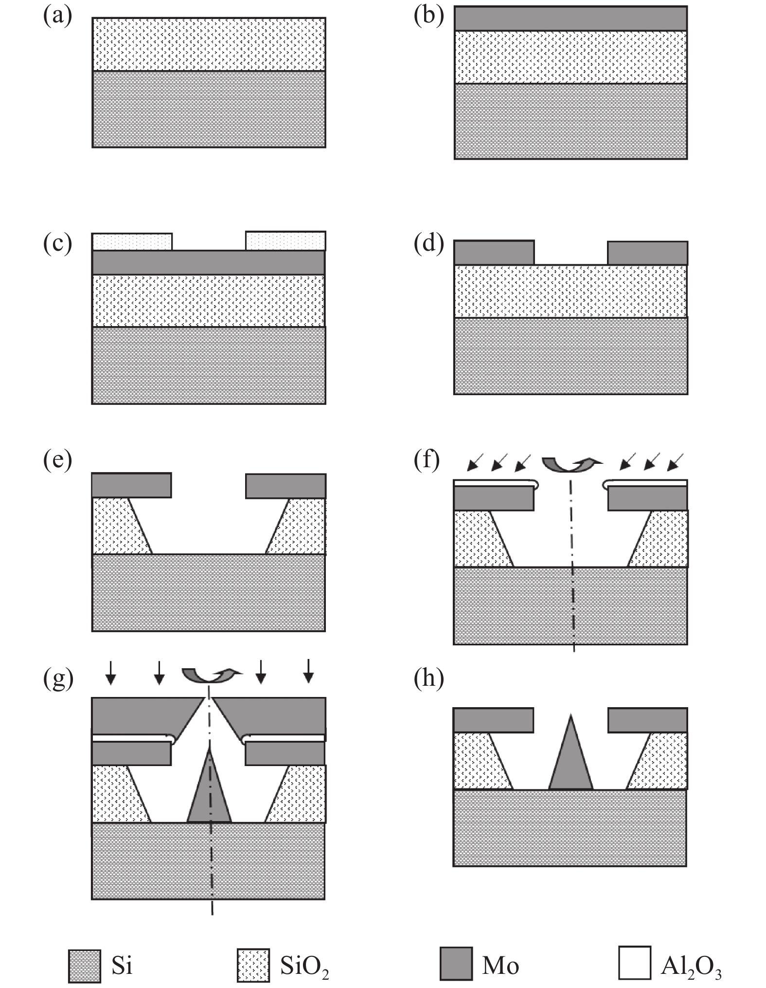
图 2 Spindt阴极制备流程图。(a)硅片热氧化,(b)栅极层沉积,(c)光刻(栅极图案化),(d)ICP刻蚀栅极,(e)湿法腐蚀绝缘层空腔,(f)沉积牺牲层,(g)尖锥沉积,(h)剥离
Figure 2. Manufacturing process of Spindt cathode. (a) Silicon oxidation, (b) gate layer deposition, (c) gate lithography, (d) gate ICP etching, (e) cavity wet etching, (f) sacrificial layer deposition, (g) tip formation, (h) peeling off
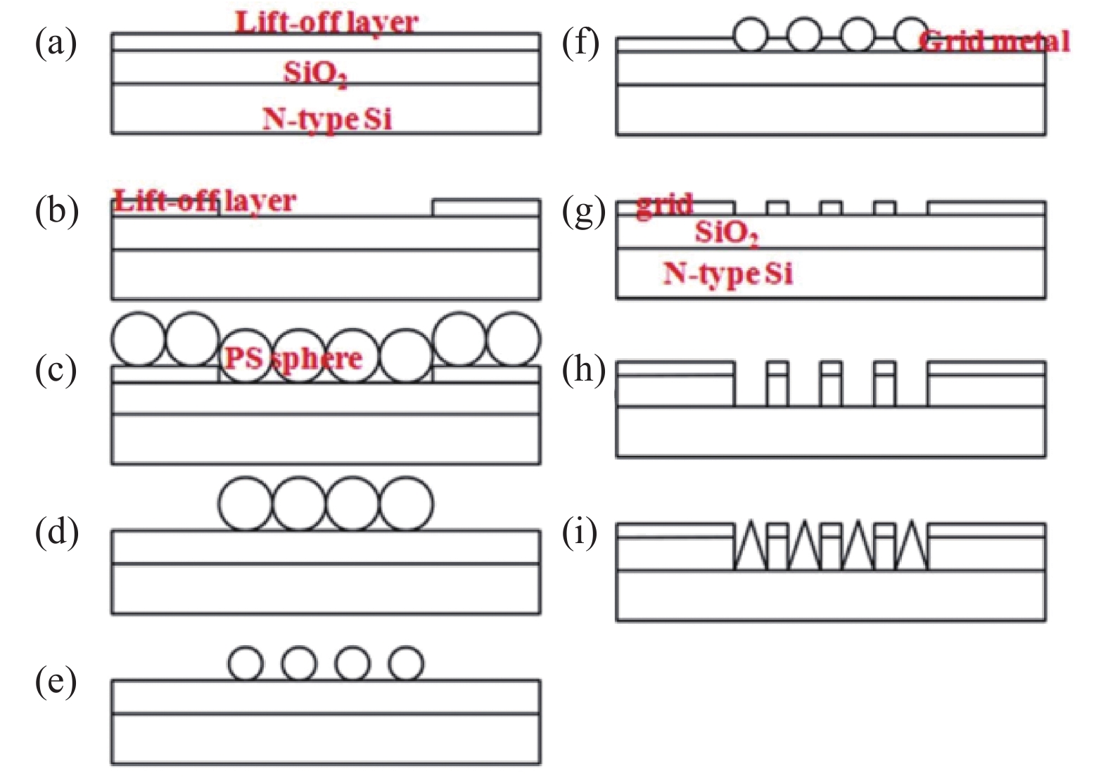
图 3 使用纳米球光刻技术制造的Spindt阴极工艺流程截面示意图。(a)沉积氧化硅和剥离层,(b)刻蚀Spindt阴极区域,(c)聚苯乙烯(PS)颗粒单层自组装,(d)移除牺牲剥离层,(e)氧反应刻蚀,(f)通过减薄的PS纳米球沉积金属薄膜,(g)移除PS纳米球,(h)从氧化层刻蚀空腔至硅基底,(i)制作发射尖
Figure 3. Cross sectional schematic of the process for fabricating Spindt cathodes using nanosphere lithography technique. (a) Silicon dioxide and sacrificial lift-off layer deposition, (b) the area of Spindt cathode etching, (c) Polystyrene (PS) particles monolayer self-assembling, (d) sacrificial lift-off layer removing, (e) oxygen reactiveion etching, (f) metal film deposition through the thinned PS nanospheres, (g) PS nanospheres removing, (h) cavities etching in the oxide down to the silicon base, (i) emission tips forming
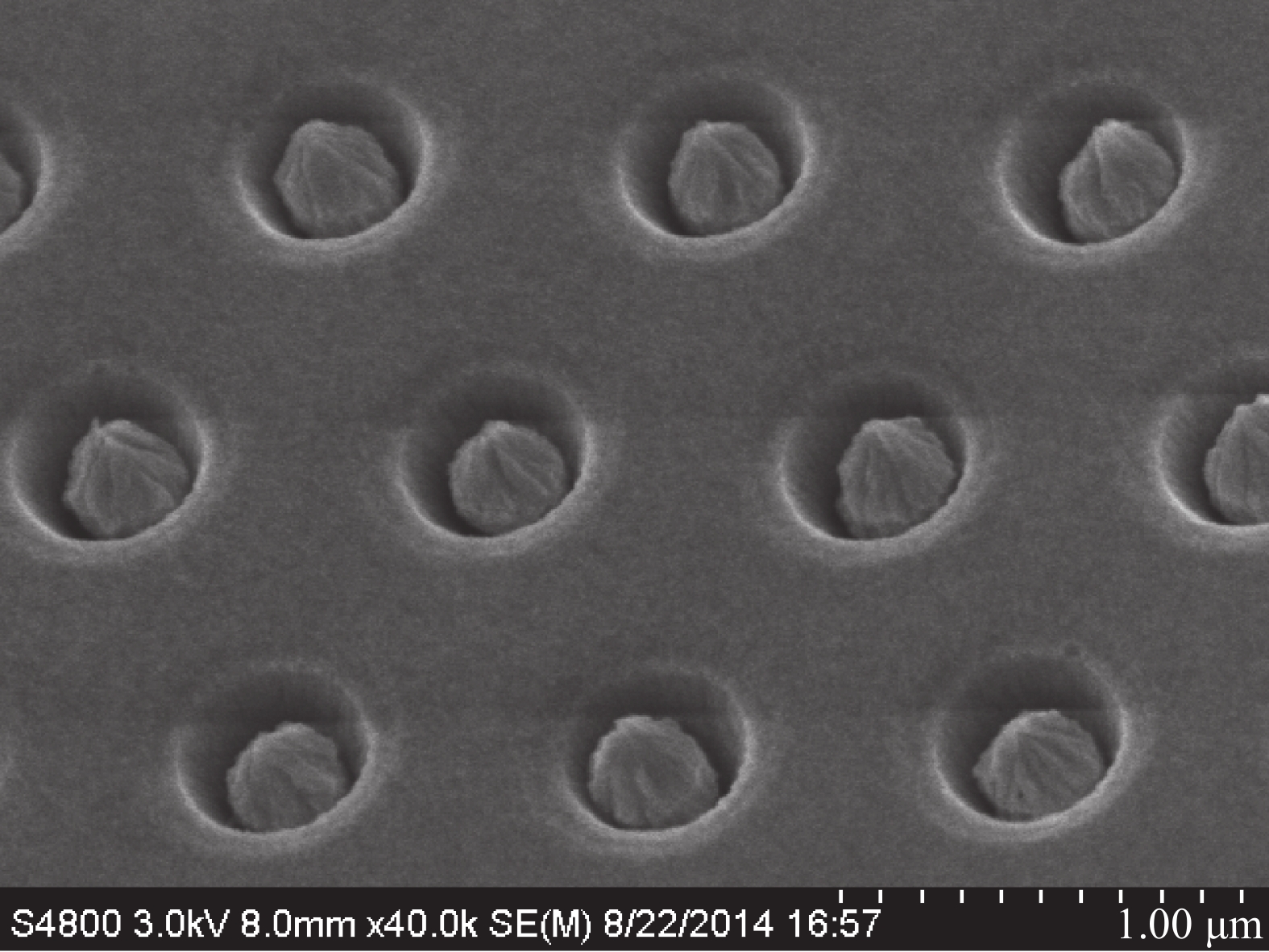
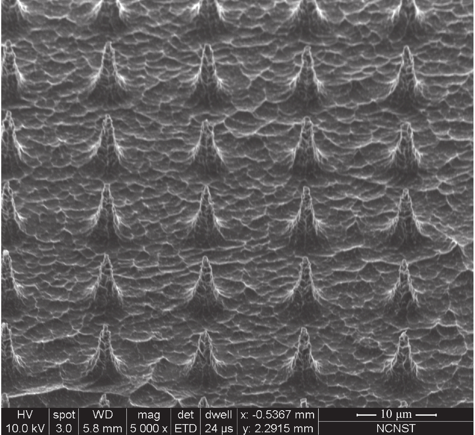
图 4 使用纳米球光刻技术制造的Spindt阴极SEM图
Figure 4. SEM image of Spindt cathode fabricated with nanosphere lithography method
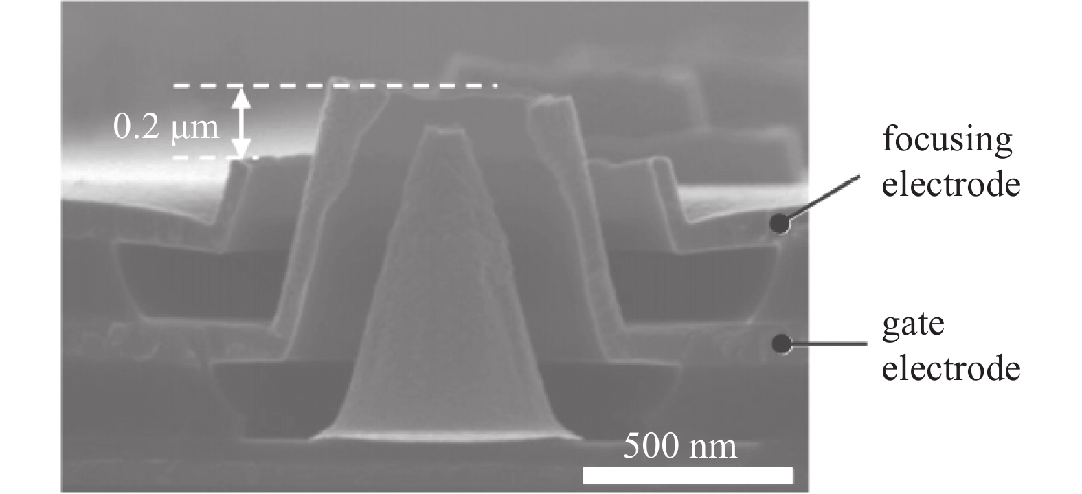
图 5 具有Ni尖端的Spindt型火山结构双栅场发射阵列截面图
Figure 5. A cross-sectional image of the Spindt-type Ni volcano-structured double-gated field emitter arrays
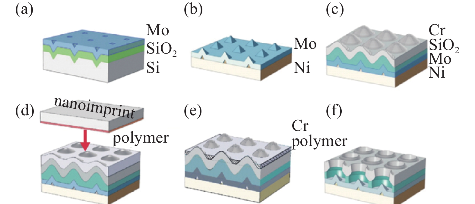
图 6 高密度栅控场发射阵列的制造工艺示意图。(a)首先用Mo填充热氧化的各向异性蚀刻的Si(100)模板,(b)随后沉积Cr/Pd晶种层和厚Ni电镀层,然后化学方法去除Si模板和热氧化物,(c)PECVD 沉积SiO2,蒸发沉积Cr和旋涂聚合物,(d)纳米压印工艺修饰软聚合物,(e)聚合物的干法刻蚀,(f)Cr栅极孔的干法刻蚀和SiO2的湿法腐蚀
Figure 6. Schematic representation of the fabrication process for the high-density gated FEAs. (a) The process started by filling the thermally oxidized anisotropically etched Si(100) template with Mo, (b) subsequent deposition of seed Cr/Pd layers and thick Ni layer electroplating, followed by chemical removal of Si template and thermal oxide. (c) deposition of PECVD SiO2, evaporation of Cr and polymer spin coating. (d) soft polymer flattering by nanoimprint process. (e) dry etch of polymer, (f) dry etch of Cr gate apertures and wet etch of SiO2
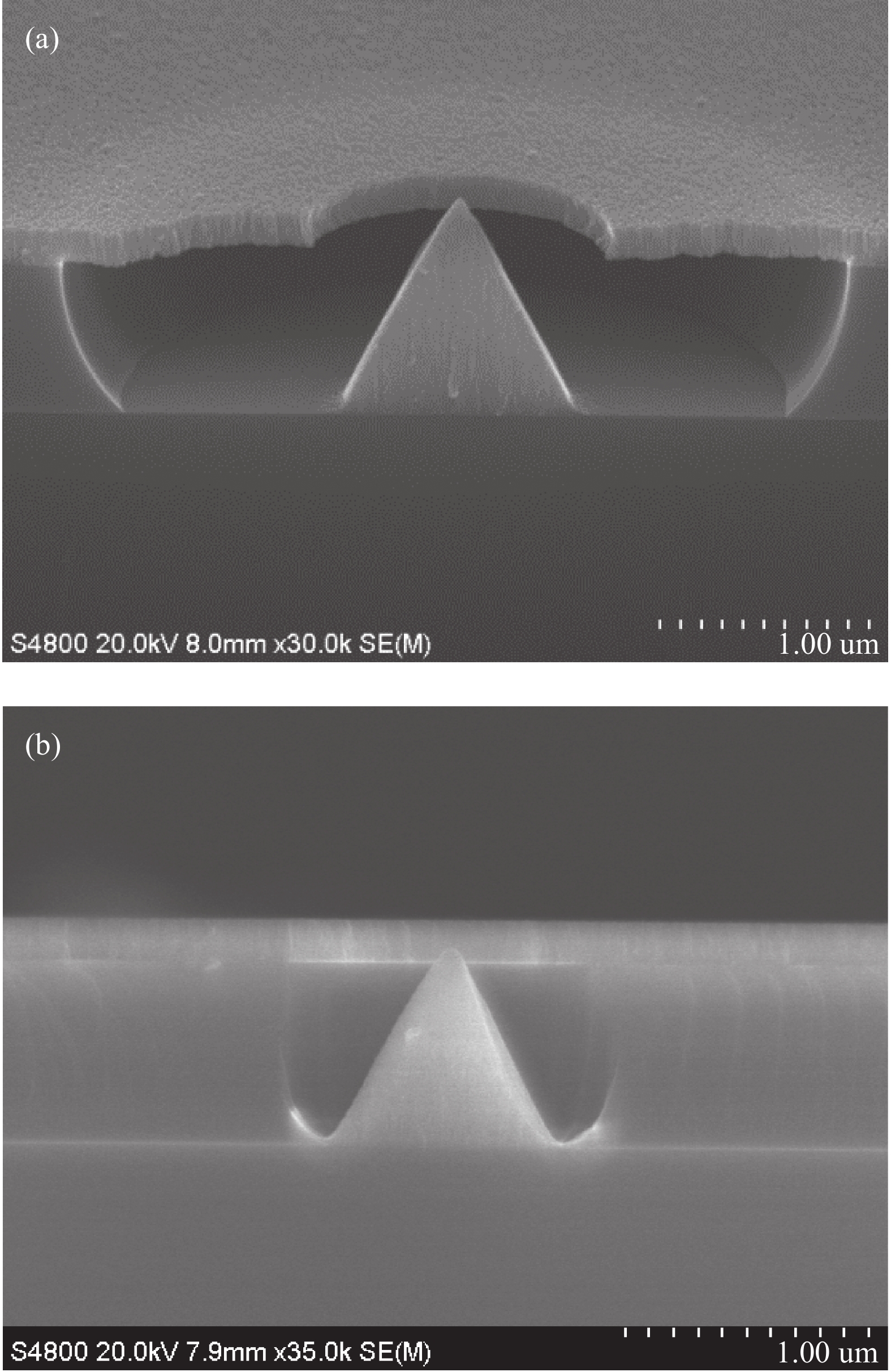
图 8 Spindt阴极绝缘层空腔断面SEM图。(a)优化前,(b)优化后
Figure 8. Cross section SEM images of the Spindt cathode insulation layer cavity. (a) Before optimization, (b) after optimization
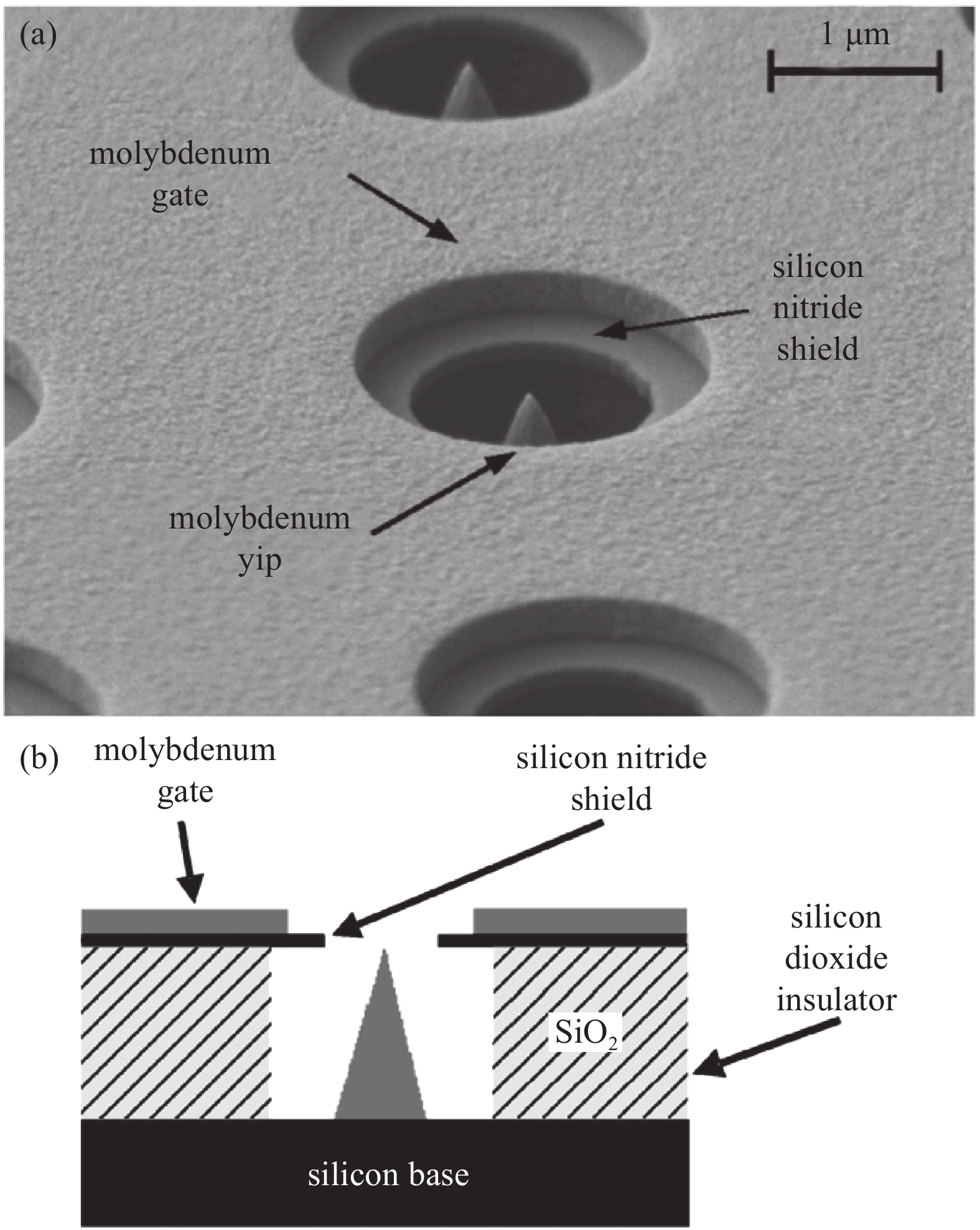
图 9 为了提高工作电压,对标准Spindt型阴极阵列进行了结构修改。(a)具有Si3N4屏蔽层的阵列的SEM图,(b)具有Si3N4介质屏蔽层的Spindt型阵列的示意图
Figure 9. The modification performed to standard Spindt-type arrays to increase the operating voltage. (a) Scanning electron micrograph of a Si3N4 shielded array, (b) schematic of the Spindt-type array with a shield of Si3N4 dielectric
图 10 多绝缘层Spindt阴极结构示意图
Figure 10. Schematic of Spindt cathode with insulating multilayer structure
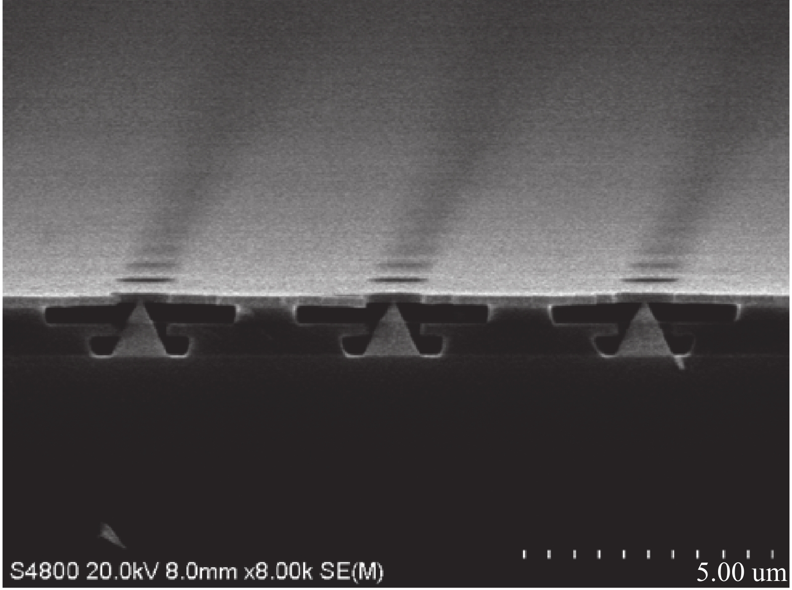
图 11 多绝缘层Spindt阴极截面图
Figure 11. Cross section of Spindt cathode with an insulating multilayer structure
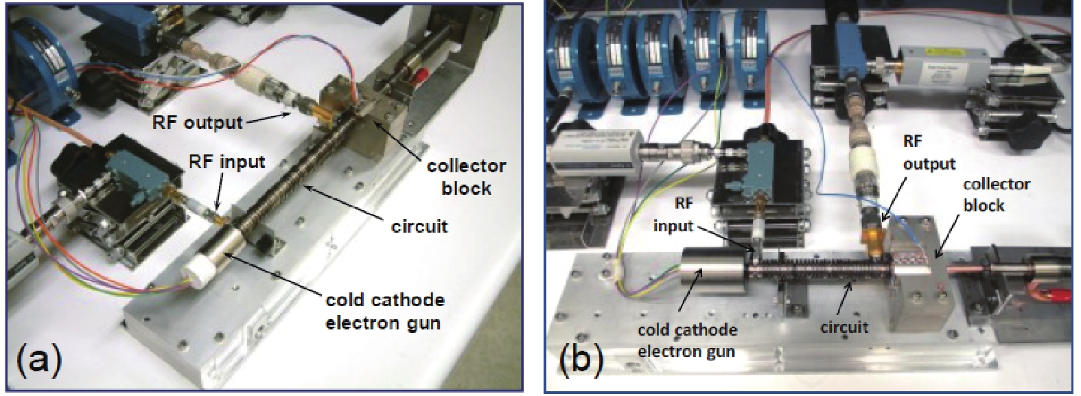
图 12 冷阴极行波管。(a)测试中的 C 波段冷阴极 TWT – 频率范围 4~6 GHz, (b)测试中的 X/Ku 波段 TWT – 频率范围 6~18 GHz
Figure 12. Traveling wave tube based cold cathode. (a) C-Band cold cathode TWT on test-frequency range 4~6 GHz, (b) X/Ku-Band TWT on test-frequency range 6~18 GHz
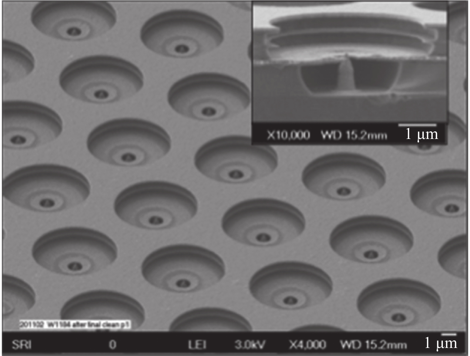
图 13 带有集成聚焦电极(IFE)的spindt 阴极阵列。插图:阵列中单个发射器的横截面
Figure 13. Array of Spindt cathodes with integral focus electrode (IFE). Inset: Cross section of an individual emitter in the array
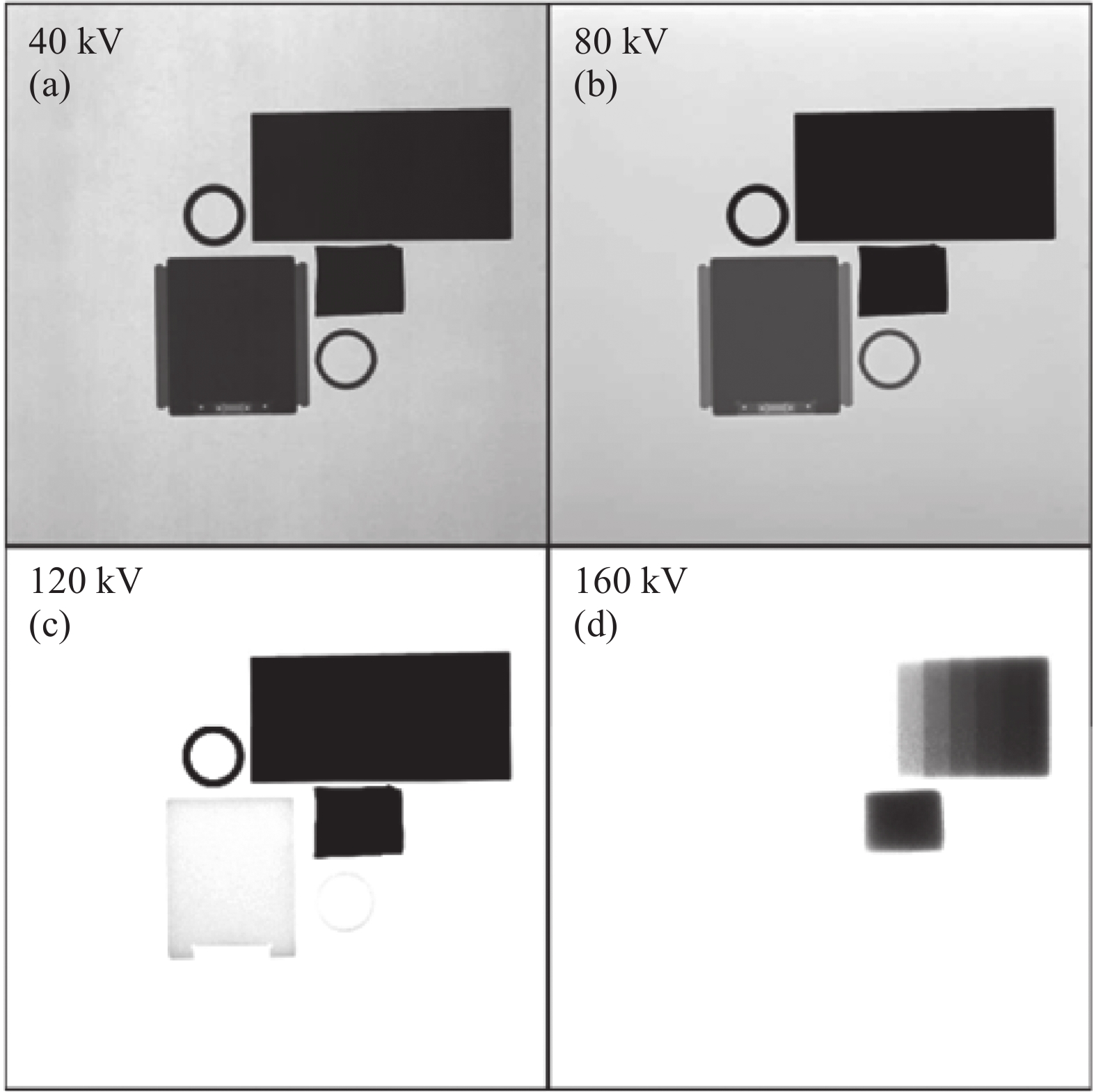
图 15 在不同能量下拍摄的不同材料的X射线图像−40(a)、80(b)、120(c)和160 kV(d)。对于每个图像,X射线曝光为5 mA阳极电流和20 ms脉冲
Figure 15. X-ray images of different materials taken at different energies – 40 (a), 80 (b), 120 (c), and 160 kV (d). For each image, the X-ray exposure was 5 mA anode current and 20 ms pulse
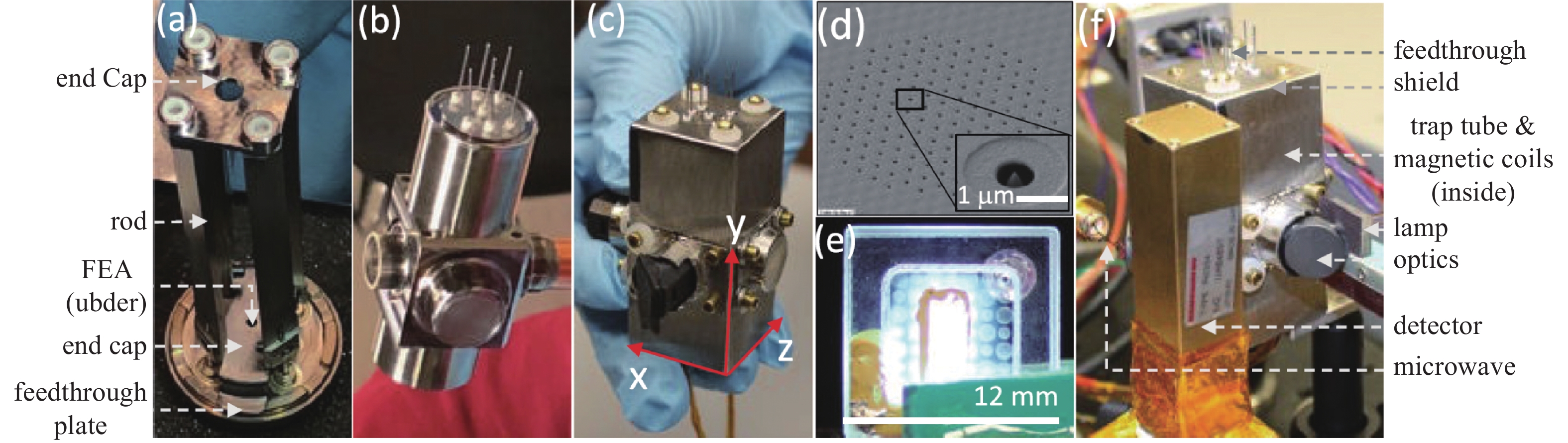
图 16 30 cc 真空管(b)中使用的线性离子阱(a)的照片,该真空阱由一层屏蔽层包围(c)。还显示了FEA的图像 (直径为50 μm的Spindt场发射阵列在包含109个尖锥的4 μm中心上的SEM图,插图:阵列中的典型发射尖端的高放大倍数图)(d)和使用的微腔等离子灯(e),集成的100 cc物理封装如(f)所示
Figure 16. Photograph of the linear ion trap used (a) in the 30-cc vacuum tube (b) enclosed by a layer of shielding (c). Also shown are an image of the FEA (SEM image of 50 μm diameter Spindt emitter array on 4 μm centers containing 109 tips. Inset: High magnification of a typical emitter tip in the array.) (d) and a microcavity plasma lamp used (e). The integrated 100-cc physics package is shown in (f)
-
[1] Shoulders K R. Microelectronics using electron-beam-activated machining techniques[J]. Advances in Computers,1961,2:135−293 [2] Spindt C A. A thin-film field-emission cathode[J]. Journal of Applied Physics,1968,39(7):3504−3505 doi: 10.1063/1.1656810 [3] Spindt C A, Brodie I, Humphrey L, et al. Physical properties of thin-film field emission cathodes with molybdenum cones[J]. Journal of Applied Physics,1976,47(12):5248−5263 doi: 10.1063/1.322600 [4] Zhu W. Vacuum microelectronics[M]. New York:John Wiley & Sons, 2001:176−177 [5] Nagao M, Yoshida T, Kanemaru S, et al. Fabrication of a field emitter array with a built-in einzel lens[J]. Japanese Journal of Applied Physics,2009,48(6S):06FK02 doi: 10.1143/JJAP.48.06FK02 [6] Nagao M, Yoshida T, Nishi T, et al. A novel fabrication of Spindt-type field emitters with focusing electrodes[C]//Proceedings of the 25th International Vacuum Nanoelectronics Conference, Jeju:IEEE, 2012:1−2 [7] Li N N, Zheng B Q, Yan F, et al. High-density gate aperture arrays for Spindt cathode fabricated using nanosphere lithography[C]//Proceedings of the 25th IEEE International Vacuum Electronics Conference, Beijing:IEEE, 2015 [8] Li N N, Yan F, Pang S C, et al. Novel nanofabricated Mo field-emitter array for low-cost and large-area application[J]. IEEE Transactions on Electron Devices,2018,65(10):4369−4374 doi: 10.1109/TED.2018.2862409 [9] Li X H, Yang C F, Feng J J, et al. Effect of ageing process on performance of molybdenum field emission arrays[J]. Applied Surface Science,2005,251(1-4):210−214 doi: 10.1016/j.apsusc.2005.03.158 [10] 李兴辉, 冯进军, 白国栋, 等. 提高钼尖锥场致发射阵列阴极发射性能的研究[J]. 液晶与显示,2004,19(5):343−348 (in Chinese) Li X H, Feng J J, Bai G D, et al. Improvement of emission performance of molybdenum field emission arrays[J]. Chinese Journal of Liquid Crystals and Displays,2004,19(5):343−348 [11] 李含雁. 涂敷ZrC薄膜的Mo-Spindt场致发射阵列阴极的研究[D]. 北京:北京真空电子技术研究所, 2006 (in Chinese) Li H Y. Research on Mo Spindt field emission array cathode coated with ZrC thin film[D]. Beijing:Beijing Vacuum Electronics Research Institute, 2006 [12] Ding M Q, Gruen D M, Auciello O, et al. Field emission properties of ultrananocrystalline diamond coated Si microtip[C]//Proceedings of the Abstracts of the 8th IUMRS International Conference on Electronic Materials IUMRS-ICEM2002, Xi'an:Chinese Materials Research Society, 2002:PT03 [13] Chalamala B R, Wallace R M, Gnade B E. Surface conditioning of active molybdenum field emission cathode arrays with H2 and helium[J]. Journal of Vacuum Science & Technology B,1998,16(5):2855−2858 [14] Schwoebel P R, Spindt C A, Holland C E. High current, high current density field emitter array cathodes[J]. Journal of Vacuum Science & Technology B,2005,23(2):691−693 [15] Bhattacharya R, Karaulac N, Rughoobur G, et al. Ultraviolet light stimulated water desorption effect on emission performance of gated field emitter array[J]. Journal of Vacuum Science & Technology B,2021,39(3):033201 [16] Bhattacharya R, Shih P C, Palacios T, et al. Field emission characteristics of GaN arrays[C]//Proceedings of the 23rd International Vacuum Electronics Conference, Monterey:IEEE, 2022:142−143 [17] Mimura H, Neo Y, Nagao M, et al. Volcano-structured double-gated field emitter arrays; emission characteristics and applications[C]//Proceedings of the 24th International Vacuum Electronics Conference, Chengdu:IEEE, 2023:572−573 [18] Neo Y, Soda T, Takeda M, et al. Focusing characteristics of double-gated field-emitter arrays with a lower height of the focusing electrode[J]. Applied Physics Express,2008,1(5):053001 [19] Neo Y, Takeda M, Soda T, et al. Emission and focusing characteristics of volcano-structured double-gated field emitter arrays[J]. Journal of Vacuum Science & Technology B,2009,27(2):701−704 [20] Itoh J, Tohma Y, Morikawa K, et al. Fabrication of double-gated Si field emitter arrays for focused electron beam generation[J]. Journal of Vacuum Science & Technology B,1995,13(5):1968−1972 [21] Wu M, Huang Y, Huang Z J, et al. Gated Si-tips with integrated ion collector for reliable and stable field electron emission[C]//Proceedings of the International Vacuum Nanoelectronics Conference, 2019 [22] Nagao M, Yoshizawa S. Fabrication of Spindt-type double-gated field-emitters using photoresist lift-off layer[C]//Proceedings of the 27th International Vacuum Nanoelectronics Conference, Engelberg:IEEE, 2014:226−227 [23] Nagao M, Gotoh Y, Neo Y, et al. Beam profile measurement of volcano-structured double-gated Spindt-type filed emitter arrays[C]//Proceedings of the 28th International Vacuum Nanoelectronics Conference, Guangzhou:IEEE, 2015:190−191 [24] Nagao M, Murakami K, Khumpuang S, et al. Fabrication of volcano structured Spindt-type field emitter arrays using Minimal Fab system[C]//Proceedings of the 31st International Vacuum Nanoelectronics Conference, Kyoto:IEEE, 2018:1−2 [25] Kirk E, Tsujino S, Vogel T, et al. Fabrication of all-metal field emitter arrays with controlled apex sizes by molding[J]. Journal of Vacuum Science & Technology B,2009,27(4):1813−1820 [26] Helfenstein P, Jefimovs K, Kirk E, et al. Fabrication of metallic double-gate field emitter arrays and their electron beam collimation characteristics[J]. Journal of Applied Physics,2012,112(9):093307 doi: 10.1063/1.4764925 [27] Mustonen A, Guzenko V, Spreu C, et al. High-density metallic nano-emitter arrays and their field emission characteristics[J]. Nanotechnology,2014,25(8):085203 doi: 10.1088/0957-4484/25/8/085203 [28] Zhu N L, Xu K S, Song L, et al. Fabrication and characterization of bulk molybdenum field emission arrays[C]//Proceedings of the 18th International Conference on Solid-state Sensors, Actuators and Microsystems, Anchorage:IEEE, 2015:1168−1171 [29] 李兴辉, 白国栋, 李含雁, 等. Spindt阴极制作中剥离层的研究[J]. 真空科学与技术学报,2013,33(4):303−308 (in Chinese) Li X H, Bai G D, Li H Y, et al. Study of lift-off layers in Spindt cathode fabrication[J]. Chinese Journal of Vacuum Science and Technology,2013,33(4):303−308 [30] Li X H, Bai G D, Li H Y, et al. A potential failure reason for Spindt cathodes in high current applications[C]//Proceedings of the IEEE International Vacuum Electronics Conference, Monterey:IEEE, 2014:509−510 [31] 李兴辉, 白国栋, 李含雁, 等. Spindt阴极金属颗粒粘附失效分析[J]. 真空科学与技术学报,2015,35(4):418−423 (in Chinese) Li X H, Bai G D, Li H Y, et al. Molybdenum-particles contamination and failures of Spindt cathode[J]. Chinese Journal of Vacuum Science and Technology,2015,35(4):418−423 [32] Han P Y, Li X H, Jiang Q, et al. Solutions for short circuit failure of Spindt cathode[C]//Proceedings of the IET Ph. D Candidates Academic Seminar (China) on Vacuum Electronics, Beijing:IET, 2021:58−61 [33] Whaley D R, Duggal R, Armstrong C M, et al. 100 W operation of a cold cathode TWT[J]. IEEE Transactions on Electron Devices,2009,56(5):896−905 doi: 10.1109/TED.2009.2015614 [34] Solano I, Reichenbach B, Schwoebel P R, et al. Field desorption ion source development for neutron generators[J]. Nuclear Instruments and Methods in Physics Research Section A:Accelerators, Spectrometers, Detectors and Associated Equipment,2008,587(1):76−81 [35] Spindt C, Holland C E, Schwoebel P R, et al. 11.1:a reliable improved Spindt cathode design for high currents[C]//Proceedings of the IEEE International Vacuum Electronics Conference, Monterey:IEEE, 2010 [36] Spindt C. A brief history Vacuum Nanoelectronics, the IVNC, and the present status of the Spindt cathode[C]//Proceedings of the 25th International Vacuum Nanoelectronics Conference, Jeju:IEEE, 2012:1−2 [37] Holland C, Schwoebel P, Todd K, et al. High-speed photo-modulated Spindt cathode for FELs[C]//Proceedings of the 26th International Vacuum Nanoelectronics Conference, Roanoke:IEEE, 2013:1−2 [38] 姜琪, 韩攀阳, 杜婷, 等. 多绝缘层结构Spindt阴极设计及工艺实现[J]. 真空电子技术,2022(4):60−66 (in Chinese) Jiang Q, Han P Y, Du T, et al. Design and fabrication of an Spindt cathode with insulating multilayer structure[J]. Vacuum Electronics,2022(4):60−66 [39] Whaley D R, Gannon B M, Heinen V O, et al. Experimental demonstration of an emission-gated traveling-wave tube amplifier[J]. IEEE Transactions on Plasma Science,2002,30(3):998−1008 doi: 10.1109/TPS.2002.801527 [40] Whaley D R, Duggal R, Armstrong C M, et al. High average power field emitter cathode and testbed for X/Ku-band cold cathode TWT[C]//Proceedings of the 14th International Vacuum Electronics Conference, Paris:IEEE, 2013 [41] Whaley D R, Armstrong C M, Holland C E, et al. Cold cathode based microwave devices for current and future systems[C]//Proceedings of the 31st International Vacuum Nanoelectronics Conference, Kyoto:IEEE, 2018:1−2 [42] Holland C E, Whaley D R, Schwoebel P, et al. Development of a self focused Spindt cathode for millimeter-wave traveling wave tubes[C]//Proceedings of the 36th International Vacuum Nanoelectronics Conference, Cambridge:IEEE, 2023 [43] Lockwood N P, Tang W, Fairchild S B. Single walled nanotube fiber cathode emission property modification and evaluation[C]//Proceedings of the International Vacuum Electronics Conference 2012, Monterey:IEEE, 2012:25−26 [44] Guiset P, Combrie S, Antoni T, et al. Optically driven field emission array for THz amplifiers[C]//Proceedings of 2009 IEEE International Vacuum Electronics Conference, Rome:IEEE, 2009:325−326 [45] 李兴辉, 白国栋, 李含雁, 等. 场发射阴极及其应用的回顾与展望[J]. 真空电子技术,2015(2):50−63 (in Chinese) Li X H, Bai G D, Li H Y, et al. Review and prospect of field emission cathodes and the applications[J]. Vacuum Electronics,2015(2):50−63 [46] Garven M, Spark S N, Cross A W, et al. Gyrotron experiments employing a field emission array cathode[J]. Physical Review Letters,1996,77(11):2320−2323 doi: 10.1103/PhysRevLett.77.2320 [47] Bandy S G, Green M C, Spindt C A, et al. Application of gated field emitter arrays in microwave amplifier tubes[C]//Proceedings of the Eleventh International Vacuum Microelectronics Conference, Asheville:IEEE, 1998:132−133 [48] Schwoebel P R, Boone J M, Shao J. Studies of a prototype linear stationary x-ray source for tomosynthesis imaging[J]. Physics in Medicine and Biology,2014,59(10):2393−2413 doi: 10.1088/0031-9155/59/10/2393 [49] Jeong U, Kang G, Lee S, et al. Revolutionizing X-Ray imaging:Spindt field emitter tube with chromatic scan capability across wide voltage range (30−160KV)[C]//Proceedings of the 36th International Vacuum Nanoelectronics Conference, Cambridge:IEEE, 2023:198−200 [50] Honda Y, Nanba M, Miyakawa K, et al. Highly sensitive HARP image sensor with Spindt-type field emitter array[C]//Proceedings of the IEEE International Nanoelectronics Conference, Sapporo:IEEE, 2014:1−4 [51] Honda Y, Takiguchi Y, Egami N, et al. Triple-gated Spindt-type FEA for image sensor with HARP target[C]//Proceedings of the 24th International Vacuum Nanoelectronics Conference, Wuppertal:IEEE, 2011:11−12 [52] Honda Y, Nanba M, Miyakawa K, et al. Electrostatic-focusing Spindt-type FEA with improved electron-beam extraction efficiency for image sensor with HARP target[C]//Proceedings of the 27th International Vacuum Nanoelectronics Conference, Engelberg:IEEE, 2014:19-20 [53] Nagao M, Gotoh Y, Neo Y, et al. Beam profile measurement of volcano-structured double-gate Spindt-type field emitter arrays[J]. Journal of Vacuum Science & Technology B,2016,34(2):02G108 [54] Honda Y, Nanba M, Miyakawa K, et al. Electrostatic-focusing image sensor with volcano-structured Spindt-type field emitter array[J]. Journal of Vacuum Science & Technology B,2016,34(5):052201 [55] Hoang T M, Chung S K, Le T, et al. Integrated physics package of micromercury trapped ion clock with 10−14-level frequency stability[J]. Applied Physics Letters,2021,119(4):044001 doi: 10.1063/5.0049734 [56] Holland C E, Prestage J D, Hoang T M, et al. Development of a micro mercury trapped ion clock prototype employing a Spindt cathode ionization source[C]//Proceedings of the 36th International Vacuum Nanoelectronics Conference, Cambridge:IEEE, 2023 -
计量
- 文章访问数: 959
- HTML全文浏览数: 959
- PDF下载数: 11
- 施引文献: 0