
 首页
首页 登录
登录 注册
注册


 下载:
下载:
-
目前,光电探测在夜视装备、光纤通信、光电传感等领域都有广泛的应用[1]。研制能够在近红外波段工作的光电探测器,是目前的一个热点课题[2-4]。负电子亲和势(NEA)光电阴极在可见光和近红外区域比传统的光电阴极如Cs3Sb、K2CsSb和Na2KSb(Cs)光电阴极具有更高的量子效率。但是,由于NEA阴极有1.2 eV的电子势垒,它们的长波阈值被限制在1.1 µm的波长内。场助光电阴极与通常的NEA光阴极相比,能显著提高长波阈值,因此在近红外光探测中有着广阔的应用前景。1974年,Bell等[5]对Ag/InP肖特基势垒光电阴极进行了场助光电发射的实验,并提出了转移电子光电发射理论,为以后的进一步研究打下了坚实的基础。Escher, Bell, Gregory等对场助光电阴极进行了大量的研究,将光电阴极的波长阈值扩展到2.1 μm(150K)[6],使其在1.55 μm下的量子效率达到了8 %[7]。日本的 M. Niigaki等在1997年首次应用PN结制作了光电阴极,其量子效率在1.3 μm处为5% [8];2014年,他们再次使用PN结结构,使阈值达到2.3 μm,这是目前为止,场助光阴极的最大波长阈值[9]。国内从20世纪80年代开始西安光学机密机械研究所对场助光电阴极的量子效率、响应时间和能带以及制备工艺进行了研究[10-15]。
量子效率是衡量光电阴极指标的一个重要因素之一,但是延长长波阈值必然以牺牲量子效率为代价。为了解决这一矛盾,本文研究了一种利用PN结并采用阵列电极实现 n- InP/p-InP/p-InGaAs的场助光阴极,并能在更长的波长阈值下实现较高的量子效率,本文对这种结构的场助光电阴极进行了理论建模,并对其性能参数进行了模拟。
-
本文设计了基于PN结的n-InP/p-InP/p-InGaAs场助光阴极,场助阴极的发射表面结构是由发射单元周期排布,其中一个发射单元的结构与能带如图1所示,主要由p-InP衬底、p-In0.53Ga0.47As吸收层、p-InP发射层、n-InP接触层以及欧姆电极构成。在阴极工作时,对其施加一个反向偏置电压,电子发射层p-InP表面会产生能带弯曲,如图1(c)所示。In0.53Ga0.47As的吸收层在近红外光照射下会吸收光子能量,形成电子空穴对,被激发到导带的光电子穿过发射层向阴极表面漂移,在发射层能带的弯曲区得到电场的加速,使其更易于进入真空。
在进行器件模拟时,常用的基本结构是 Poisson方程和电流连续性方程,在光照和电场作用下,载流子会发生扩散和漂移,并且载流子浓度是位置(x,y)的函数。依据半导体载流子输运规律,场助阴极的光生载流子二维连续性方程表示为:
式中,Dn(x,y)和Dp(x,y)为电子与空穴的扩散系数,n(x,y)和p(x,y)分别为电子与空穴浓度,μn(x,y)和μp(x,y)分别为电子和空穴的迁移率,En(x,y)和Ep(x,y)分别为电子和空穴在p-InGaAs吸收层和p-InP发射层内部受到的电场大小,U(x,y)为载流子复合速率,G(x,y)为光电子产生函数,2y1为发射面宽度,y2-y1为欧姆电极宽度。
光电子产生函数G(x,y)由下式描述:
式中,I0为入射光强度,R为阴极材料对入射光的反射率,α为光子吸收系数。
在计算泊松方程、电流连续性方程时,N-InP/p-InP/p-InGaAs场助阴极理论模型的边界主要由欧姆接触边界和p-InP发射层上的发射面边界组成。
场助阴极的n-InP接触层采用重掺杂,能与金属形成欧姆接触。欧姆接触的界面上没有势垒[16],并且具有很低的寄生电阻,使得载流子能够自由地穿过。当n-InP接触层和电极欧姆接触时,其边界条件是:
当光电子在阴极表面输运时,由于电子的逸出概率影响,有一些会被发射到真空中,而另一些则会被复合,从理论上说阴极表面的电子浓度为0,所以发射面边界条件为[17]:
量子效率是表现光电阴极性能的一种形式,分为内量子效率和外量子效率,本文主要关注外量子效率,即器件最终发射出来的电子数与光源的源光子数之比[18]。本文通过计算光电阴极的光谱响应从而得到阴极的外量子效率。若照射到阴极面上的单色入射光的辐射功率为W(λ),阴极产生的光电流为I(λ),则阴极的光谱灵敏度为:
把照射到阴极的单色光的灵敏度S(λ)连成一条曲线,就是光谱响应曲线,光谱响应与量子效率之间的转换公式为:
式中c为光速,h为普朗克常数,e是电子电荷量,λ为入射单色光的波长,单位为nm,光谱灵敏度S(λ)的单位是mA/W。
此外,当电子到达发射面时,其表面的清洁度、激活层质量等因素会对电子逸出几率产生一定的影响,若将电子逃逸几率定义为P,则实际量子效率应用下式表示:
本文中设定电子逸出几率为1。
-
为了确定n-InP/p-InP/p-InGaAs场助光阴极的最佳参数范围,模拟了p-InP衬底、p-In0.53Ga0.47As吸收层、p-InP发射层、n-InP接触层的厚度和掺杂浓度以及基极(Wb)的宽度和每个发射单元表面(We)的宽度。由于场助阴极的发射表面结构是一个由基底分隔的周期结构,因此本文模拟了一个场助阴极单元的发射特性。
-
电子扩散系数会影响电子输运,而电子扩散系数又会受到掺杂浓度影响。当光照射阴极表面时,p-In0.53Ga0.47As吸收层将吸收光子能量,形成电子空穴对,而后光电子向表面输运。如图2 (a),不同偏压下量子效率随吸收层掺杂浓度变化曲线所示,可以看到量子效率随吸收层掺杂浓度的增加呈现先增加后减小的趋势[19],且偏压越大,增加和减小的趋势越明显,为了尽量增加阴极整体耗尽区的宽度,使更多的光电子输运到发射层,吸收层掺杂浓度不能太高,故选择5×10¹⁷/cm3作为吸收层掺杂浓度[17]。
发射层掺杂浓度的大小会影响电子的输运和阴极表面的电子逸出几率。如图2 (b)所示,为不同电压下量子效率随发射层掺杂浓度变化曲线,结果表明,量子效率随发射层掺杂浓度增加,先增大到一定峰值而后急剧下降。这是由于电子的扩散长度会因为掺杂浓度过高会迅速缩短,在到达阴极表面之前,电子就会在导带底部发生热化,从而使到达阴极表面的电子数目减少。所以发射层掺杂浓度不能太高,考虑激活工艺的实现,选择发射层浓度为2.2×10¹⁸ /cm3左右。
接触层的掺杂浓度对电子的输运没有明显的影响,但在较高的掺杂浓度下,欧姆接触容易形成。如图2 (c)所示,为不同电压下量子效率随接触层掺杂浓度变化曲线,结果表明,量子效率随着接触层掺杂浓度的增加,也会先增大而后减小,并在1×10¹⁹ /cm−3处出现峰值,考虑到欧姆接触以及掺杂工艺,将接触层掺杂浓度定为1×1019 /cm−3。
-
在n-InP/p-InP/p-InGaAs场助光阴极外延层中,p-In0.53 Ga0.47As的吸收层中的光电子被激发并输送至表面,其中一些到达发射层后被发射到真空中,而另外一些则通过p-InP发射层和n-InP接触层所形成的耗尽区,从而由电极所收集。所以外延层各层的厚度对电子的产生和传输都有很大的影响。
吸收层厚度增加,量子效率也会增加,但吸收层厚度变大也会增加电子的输运距离,从而使阴极响应时间也会增加,所以吸收层的厚度不能太高或太低。如图3(a)所示,量子效率随吸收层厚度增大呈现先增加后微弱减小的趋势,综合考虑,阴极吸收层厚度可以设置为3 μm。
发射层的厚度是影响阴极量子效率的关键因素,发射层的厚度过大,使表面能带不能发生弯曲,从而使光子不能到达发射层发射出去,为了得到更好的激活效果和电子在发射层更好地加速,发射层也不能太薄[20]。如图3(b)所示,量子效率随发射层厚度的增加先增大后减小,而且量子效率峰值所对应的发射层厚度会随电压的减小而减小,因为发射层厚度越大则能带越难弯曲,所以反偏电压也应变大从而提供更大的电场使能带弯曲。综合考虑发射层厚度设置为25 nm。
n-InP接触层的目的有主要有两个,一是与p-InP发射层形成PN结,二是与电极形成欧姆接触,保证良好的电压接触,所以它的厚度对量子效率的影响不大。如图3(c)经过仿真发现量子效率随接触层厚度增加几乎不变,所以综合考虑到阴极制备工艺的可实现性,接触层厚度可以设定为0.2 μm。
-
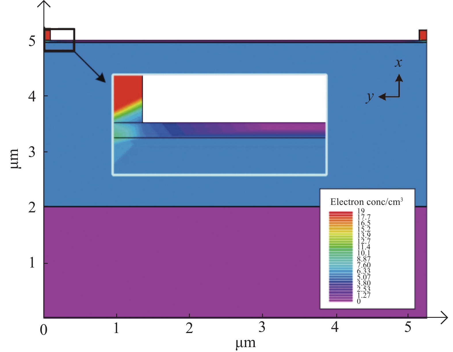
量子效率与表面发射结构直接相关,场助光电阴极电子浓度分布如图4所示,大部分电子被电极收集,只有少数电子从发射面发射出去。如果电极宽度很窄,不能提供足够的电场,而发射面宽度过宽,远离电极的发射面处的能带无法弯曲,发射出去电子数量则会减少,而电极宽度过宽,电极会收集大部分的电子,会影响从发射面发射出去的电子数量[21]。
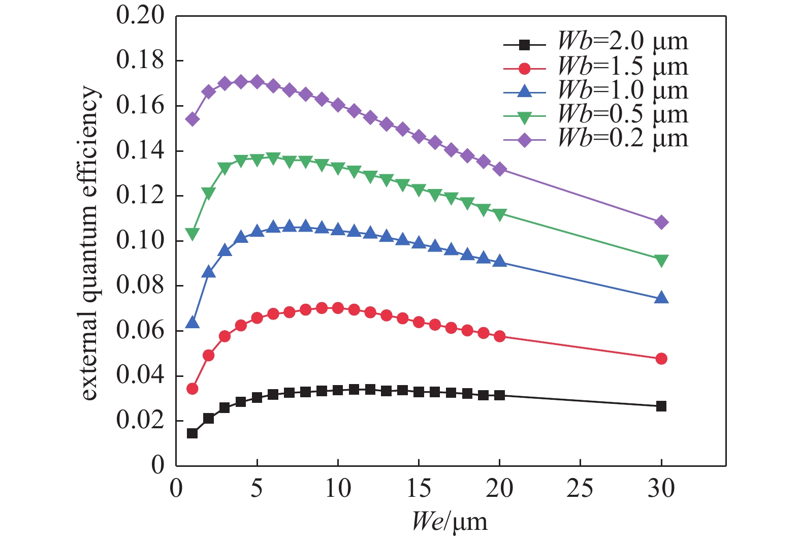
采用上文仿真得到的最佳参数进行仿真:n-InP接触层的掺杂浓度为1×10¹⁹ /cm3,厚度为0.2 μm 、p-InP发射层的掺杂浓度为2.2×10¹⁸ /cm3,厚度为25 nm、p-InGaAs吸收层的掺杂浓度为5×10¹⁷ /cm3,厚度为3 μm,如图5所示,在5 V偏压下,量子效率随发射面宽度we的增大先增加后减小,量子效率的峰值大概在发射面宽度为5~8 μm左右,且随着电极宽度Wb的减小,量子效率会不断增大,且在电极宽度为0.2 μm、发射面宽度为5 μm时,得到量子效率峰值为17.2%。出于对量子效率和工艺制备难度的考虑,电极宽度可以设置为1~2 μm,发射面宽度设置为5~8 μm。
-
综上所述,本文建立了n-InP/p-InP/p-InGaAs场助光阴极的电子发射模型,并在此基础上进行了理论模拟。依据模拟结果和制备工艺的限制,给出了p-InP衬底、p-In0.53Ga0.47As吸收层、p-InP发射层、n-InP接触层的厚度和掺杂浓度以及基极的宽度和每个发射单元表面宽度的最佳范围,在5 V偏压下1.55 μm处的外量子效率为17.2%,为场助光电阴极的结构设计和应用提供了理论基础。场助光电阴极有效解决了传统光电阴极在较长波长阈值处量子效率低的问题,而且PN结结构可以承受比肖特基接触更高的温度且不会影响PN结的整流特性,在夜视设备、光探测设备以及条纹相机领域发展潜力很大,场助光电阴极的研究将会促进近红外光电探测技术的发展。
n-InP/p-InP/p-InGaAs场助光电阴极理论建模与仿真
Theoretical Modeling and Simulation of n-InP/p-InP/p-InGaAs Field-Assisted Photocathode
-
摘要: 场助光电阴极与通常的负电子亲和势光阴极相比,能显著延长长波阈值,因此在近红外光探测中有着广阔的应用前景。本文利用二维连续性方程建立了n-InP/p-InP/p-InGaAs场助光阴极的电子发射模型。通过模型模拟得到了电子发射电流,并计算了外量子效率。分析了不同偏压下外延层的掺杂浓度和厚度对量子效率的影响,根据仿真结果及制备条件限制,确定了阴极外延结构的最佳参数:n-InP接触层的掺杂浓度为1×1019 /cm3,厚度为0.2 μm ;p-InP发射层的掺杂浓度为2.2×10¹⁸ /cm3,厚度为25 nm;p-InGaAs吸收层的掺杂浓度为5×10¹⁷ /cm3,厚度为3 μm。对电极和发射面的宽度进行了模拟,发射单元表面的宽度最佳范围为5~8 μm,并分析了不同偏压下电极宽度和发射面宽度对量子效率的影响。为场助光电阴极的结构设计和应用提供了理论基础,有利于场助光电阴极的制备。n-InP/p-InP/p-InGaAs场助光电阴极有效提高了发射电流效率,室温5 V偏压下外量子效率在1.55 μm处最大值为17.2%。Abstract: Compared with the common negative electron affinity photocathode, the field-assisted photocathode can significantly extend the long-wavelength threshold, so it has a broad application prospect in near-infrared light detection. In this work, the electron emission model of n-InP/p-InP/p-InGaAs field-assisted photocathode was established by using the two-dimensional continuity equations. The electron emission current was obtained by model simulation, and the external quantum efficiency was calculated. The influence of the doping concentration and thickness of the epitaxial layer on the quantum efficiency under different bias voltages was analyzed. According to the simulation results and the limitations of the preparation conditions, the optimal parameters of the cathode epitaxial structure were determined: the doping concentration and the thickness of the n-InP contact layer are 1×10¹⁹/cm3 and 0.2 μm, respectively; the doping concentration and the thickness of the p-InP emission layer are 2.2×10¹⁸/cm3 and 25 nm, respectively; the doping concentration and the thickness of the p-InGaAs absorber layer are 5×10¹⁷/cm3 and 3 μm, respectively. The widths of the electrode and the emission surface were simulated, and the optimal range of the width of the surface of the emitting unit was 5~8 μm, and the effects of the electrode width and the width of the emission surface on the quantum efficiency under different bias voltages were analyzed. Simulation results provide a theoretical basis for the structure design and applications of the field-assisted photocathode and are beneficial to the preparation of the field-assisted photocathode. The n-InP/p-InP/p-InGaAs field-assisted photocathode effectively improves the emission current efficiency, and the external quantum efficiency reaches a maximum of 17.2% at 1.55 μm under a 5 V bias at room temperature.
-
Key words:
- Photocathode /
- Quantum efficiency /
- Field assisted /
- InGaAs .
-

-
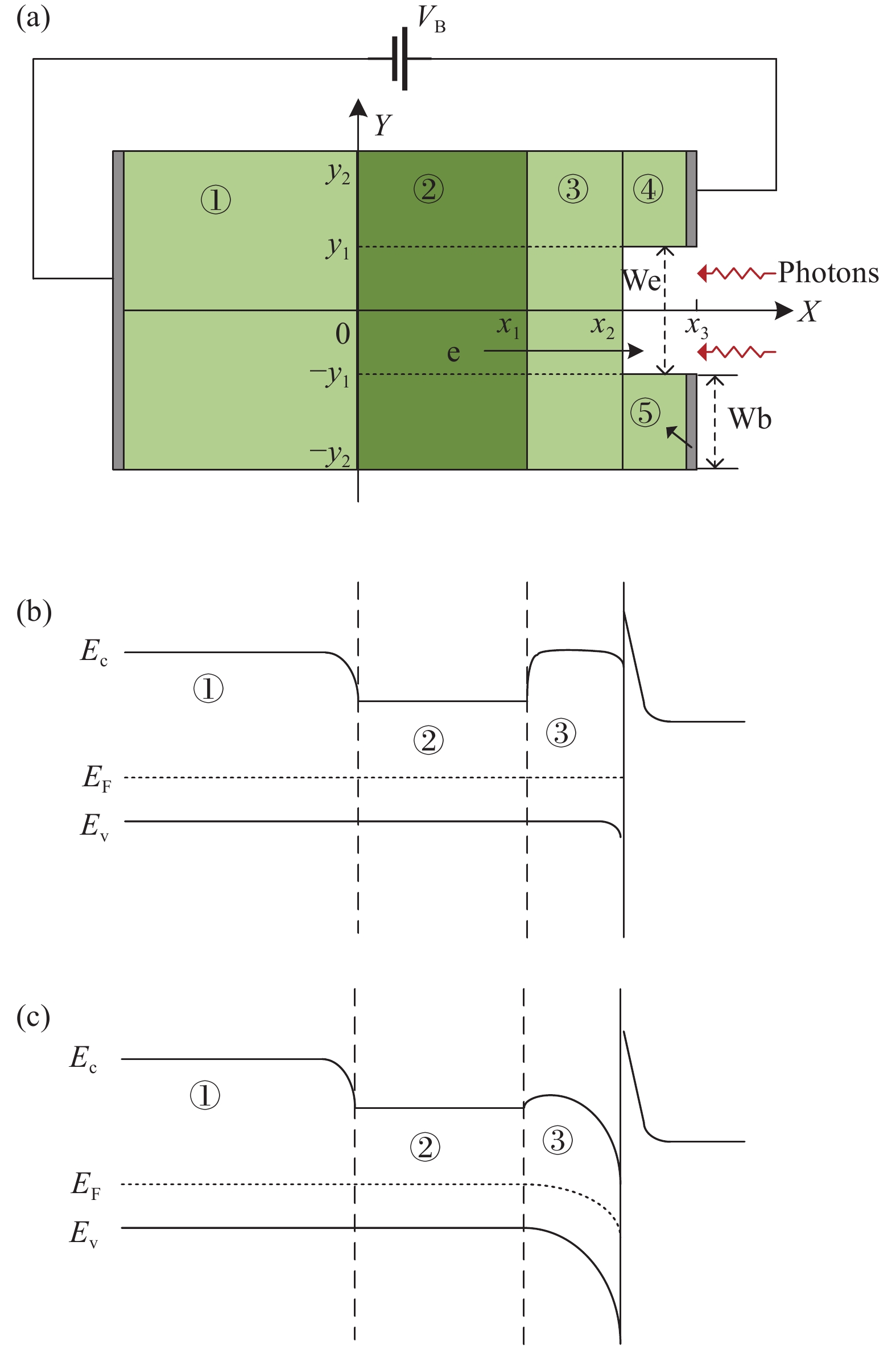
图 1 n-InP/p-InP/p-InGaAs异质结场助光阴极结构能带图。(a)阴极结构图,(b)未加偏压能带图,(c)加偏压能带图(①为p-InP衬底;②为p-In0.53Ga0.47As吸收层;③为p-InP发射层;④为n-InP接触层;⑤为电极)
Figure 1. Structure and energy band diagram of n-InP/p-InP/p-InGaAs heterojunction field photocathode. (a) cathode structure, (b) unbiased band, (c) biased band (① p-InP substrate; ② p-In0.53Ga0.47As absorption layer; ③ p-InP emission layer; ④ n-InP contact layer; ⑤ electrode)
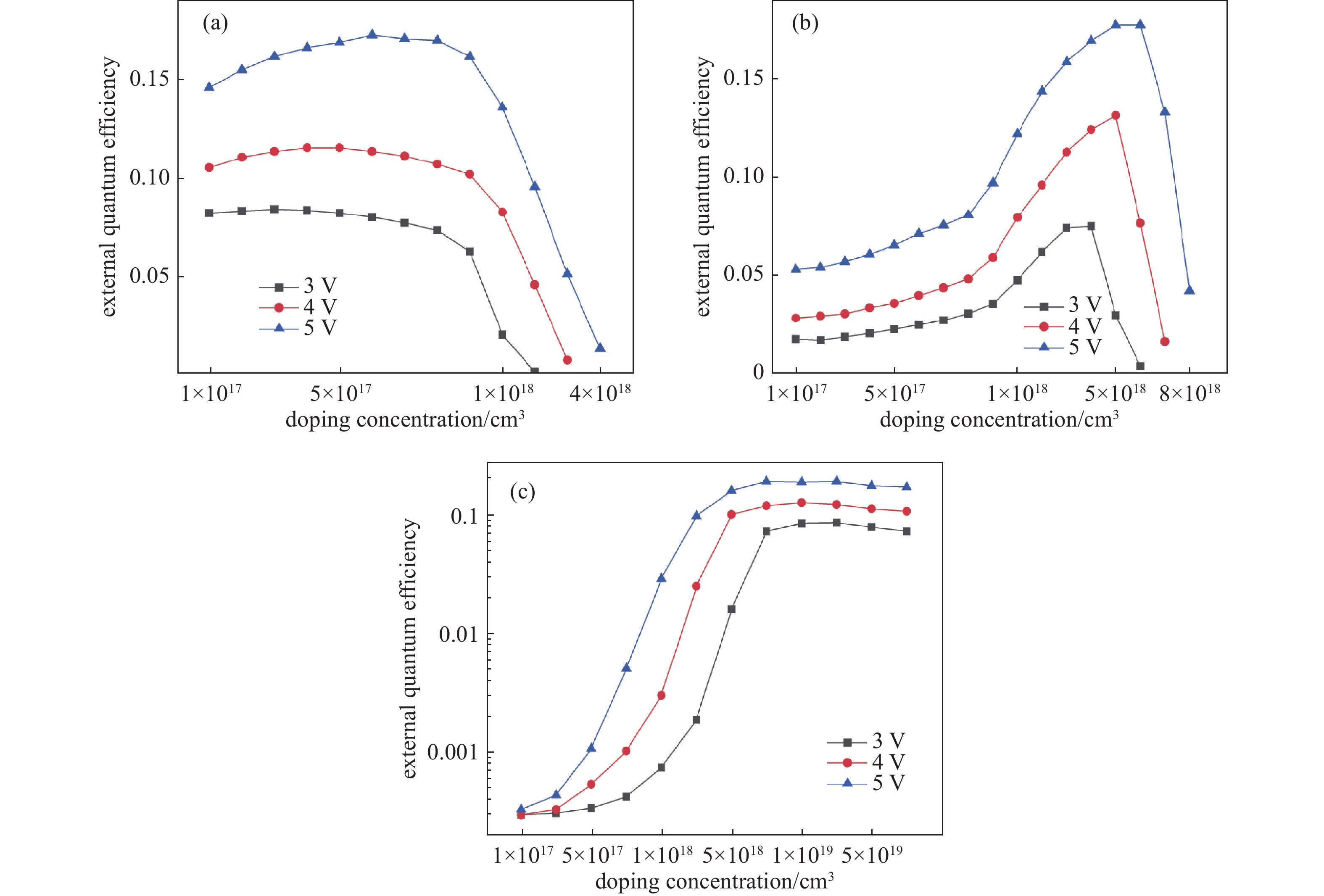
图 2 不同偏压下各层掺杂浓度对量子效率的影响。(a)吸收层,(b)发射层,(c)接触层
Figure 2. The influence of doping concentration of each layer on quantum efficiency under different bias voltage. (a) Absorption layer, (b) emission layer, (c) contact layer
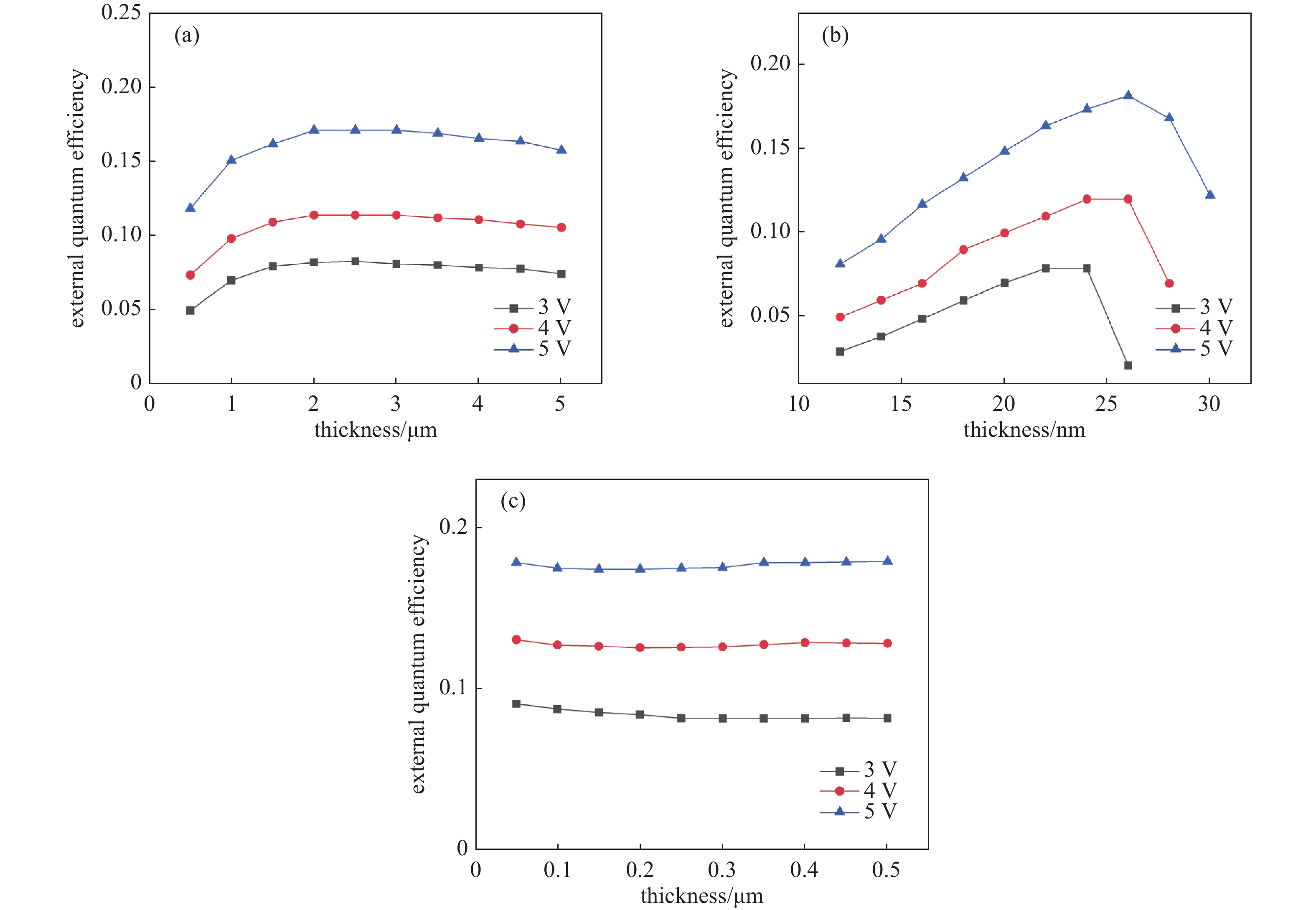
图 3 不同偏压下各层掺杂浓度对量子效率的影响。(a)吸收层,(b)发射层,(c)接触层
Figure 3. The influence of doping concentration of each layer on quantum efficiency under different bias voltage. (a) Absorption layer, (b) emission layer, (c) contact layer
-
[1] Luo M,Bai T,Guo H. Development of photocathode and device of near-shortwave infrared extension[J]. International Symposium on Photoelectronic Detection and Imaging 2013:Low-Light-Level Technology and Applications. SPIE,2013,8912:95−101 [2] Egorenkov A A,Zubkov V I. Investigation of the quantum efficiency degradation over time for InGaAs photocathodes in hybrid devices for near infrared spectral range[J]. Journal of Physics:Conference Series. IOP Publishing,2021,1799(1):012007 doi: 10.1088/1742-6596/1799/1/012007 [3] Chen L,Shen Y,Yang X,et al. Research on Cs/O activation process of near-infrared In0.53Ga0.47As photocathodes[J]. Journal of Alloys and Compounds,2020,831:154869 doi: 10.1016/j.jallcom.2020.154869 [4] Егоренков А А,Зубков В И,Соломонов А В,et al. Гибридный матричный фотоприемник для ИК-области спектра[J]. Известия СПбГЭТУ ЛЭТИ,2021(4):15−22 [5] Bell R L,James L W,Moon R L. Transferred electron photoemission from InP[J]. Applied Physics Letters,1974,25(11):645−646 doi: 10.1063/1.1655343 [6] Gregory P E,Escher J S,Saxena R R,et al. Field‐assisted photoemission to 2.1 microns from a Ag/p‐In0.77Ga0.23As photocathode[J]. Applied Physics Letters,1980,36(8):639−640 doi: 10.1063/1.91608 [7] Escher J S,Bell R L,Gregory P E,et al. Field-assisted semiconductor photoemitters for the 1—2 μm range[J]. IEEE Transactions on Electron Devices,1980,27(7):1244−1250 doi: 10.1109/T-ED.1980.20015 [8] Niigaki M,Hirohata T,Suzukki T,et al. Field-assisted photoemission from InP/InGaAsP photocathode with p/n junction[J]. Applied physics letters,1997,71(17):2493−2495 doi: 10.1063/1.120098 [9] Niigaki M,Hirohata T,Mimura H. Room temperature photoemission up to a wavelength threshold of 2.3 μm from n+-InAs0.4P0.6/p−-InAs0.4P0.6/p−-ln0.7Ga0.3As field-assisted photocathode[J]. Applied Physics Express,2014,7(11):112201−112201 doi: 10.7567/APEX.7.112201 [10] Zhou Z H,Xu X Y,Liu H L,et al. High quantum efficiency InP/In_ (0.53)Ga_ (0.47) As/InP infrared photocathode simulation[J]. Infrared and Laser Engineering,2019,48(02):247−253 (周振辉,徐向晏,刘虎林,等. 高量子效率InP/In_(0.53)Ga_(0.47)As/InP红外光电阴极模拟[J]. 红外与激光工程,2019,48(02):247−253(in chinese) Zhou Z H, Xu X Y, Liu H L, et al. High quantum efficiency InP/In_ (0.53)Ga_ (0.47) As/InP infrared photocathode simulation[J]. Infrared and Laser Engineering, 2019, 48(02): 247-253 [11] Sun Q X,Xu X Y,An Y B,et al. Simulation study on time response characteristics of InP/InGaAs/InP infrared photocathode[J]. Infrared and Laser Engineering,2013,42(12):3163−3167 (孙巧霞,徐向晏,安迎波,等. InP/InGaAs/InP红外光电阴极时间响应特性的模拟研究[J]. 红外与激光工程,2013,42(12):3163−3167(in chinese) Sun Q X, Xu X Y, An Y B, et al. Simulation study on time response characteristics of InP/InGaAs/InP infrared photocathode[J]. Infrared and Laser Engineering, 2013, 42(12): 3163-3167 (in chinese) [12] Li J M,Guo L H,Hou X. Theoretical calculation of quantum efficiency for field-assisted InP/InGaAsP semiconductor photocathodes[J]. Acta Physica Sinica,1992,41(10):1672−1678 (李晋闽,郭里辉,侯洵. 场助InP/InGaAsP半导体光电阴极量子效率的理论计算[J]. 物理学报,1992,41(10):1672−1678(in chinese) doi: 10.7498/aps.41.1672 Li J M, Guo L H, Hou X. Theoretical calculation of quantum efficiency for field-assisted InP/InGaAsP semiconductor photocathodes[J]. Acta Physica Sinica, 1992, 41(10): 1672-1678 (in chinese) doi: 10.7498/aps.41.1672 [13] Li J M,Guo L H,Wang C R,et al. Calculation of heterojunction conduction band for a field-assisted InP/InGaAsP/InP semiconductor photocathodes[J]. Acta Optica Sinica,1992,12(9):830−834 (李晋闽,郭里辉,王存让,等. 场助InP/InGaAsP/InP半导体光电阴极异质结能带的计算[J]. 光学学报,1992,12(9):830−834(in chinese) Li J M, Guo L H, Wang C R, et al. Calculation of heterojunction conduction band for a field-assisted InP/InGaAsP/InP semiconductor photocathodes[J]. Acta Optica Sinica, 1992, 12(9): 830-834 (in chinese) [14] Li Jinmin,Guo L H,Hou X. et al. Field-assisted semiconductor phontcathode with InGaAsP/InP heterojunction[J]. Acta Optica Sinica,1992,12(6):528−532 (李晋闽,郭里辉,侯洵,等. 场助InGaAsP/InP异质结半导体光电阴极的研究[J]. 光学学报,1992,12(6):528−532(in chinese) Li Jinmin, Guo L H, Hou X. et al. Field-assisted semiconductor phontcathode with InGaAsP/InP heterojunction[J]. Acta Optica Sinica, 1992, 12(6): 528-532 (in chinese) [15] Li X M,Hou X,Cheng J,et al. TE photocathode fabrication technology[J]. Semiconductor Technology,1995,8(4):26−28 (李相民,侯洵,程军,等. TE光电阴极制作技术的研究[J]. 半导体技术,1995,8(4):26−28(in chinese) Li X M, Hou X, Cheng J, et al. TE photocathode fabrication technology[J]. Semiconductor Technology, 1995, 8(4): 26-28 (in chinese) [16] Wang X B,Zhang J,Yang J,et al. Performance analysis of 2DEG in mixed polarity GaN-based HEMT[J]. Chinese Journal of Vacuum Science and Technology,2017,37(04):394−399 (王现彬,张晶,杨洁,等. 混合极性GaN基HEMT中2DEG性能分析[J]. 真空科学与技术学报,2017,37(04):394−399(in chinese) Wang X B, Zhang J, Yang J, et al. Performance analysis of 2DEG in mixed polarity GaN-based HEMT[J]. Chinese Journal of Vacuum Science and Technology, 2017, 37(04): 394-399 (in chinese) [17] Liu Y Z,Moll J L,Spicer W E. Quantum yield of GaAs semitransparent photocathode[J]. Applied Physics Letters,1970,17(2):60−62 doi: 10.1063/1.1653309 [18] 李敏. NEA光电阴极光谱响应特性研究[D]. 南京理工大学, 2004 Li M. Study on spectral response characteristics of NEA photocathode[D]. Nanjing University of Technology, 2004 [19] Cai Z P,He J F,Yao J C,et al. Band structure design and simulation of linear-doping grading layer for InGaAs/InP field-assisted pothocathode[J]. Journal of Shaanxi University of Technology(Natural Science Edition),2017,33(2):87−92 (蔡志鹏,何军锋,姚军财,等. 渐变层线性掺杂的InGaAs/InP场助阴极的能带结构设计与仿真[J]. 陕西理工学院学报(自然科学版),2017,33(2):87−92(in chinese) Cai Z P, He J F, Yao J C, et al. Band structure design and simulation of linear-doping grading layer for InGaAs/InP field-assisted pothocathode[J]. Journal of Shaanxi University of Technology(Natural Science Edition), 2017, 33(02): 87-92 (in chinese) [20] Liu F,Shi F,Jiao G C,et al. Design and simulation of p-InGaAs/p-InP heterojunction of short-wave infrared threshold field-assisted photocathode[J]. Infrared Technology,2015,37(9):778−782 (刘峰,石峰,焦岗成,等. 短波红外阈场助式光电阴极p-InGaAs/p-InP异质结设计与仿真[J]. 红外技术,2015,37(9):778−782(in chinese) Liu F, Shi F, Jiao G C, et al. Design and simulation of p-InGaAs/p-InP heterojunction of short-wave infrared threshold field-assisted photocathode[J]. Infrared Technology, 2015, 37(09): 778-782 (in chinese) [21] Wang G Y,Fu R G,Yang M Z,et al. Theoretical study on energy conversion of thermally enhanced photoemission of reflective gaas photocathode[J]. Chinese Journal of Vacuum Science and Technology,2018,38(9):779−785 (王贵圆,富容国,杨明珠,等. 反射式GaAs光电阴极的热增强光电发射能量转换理论研究[J]. 真空科学与技术学报,2018,38(9):779−785(in chinese) Wang G Y, Fu R G, Yang M Z, et al. Theoretical Study on Energy Conversion of Thermally Enhanced Photoemission of Reflective GaAs Photocathode[J]. 2018, 38(09): 779-785 -
计量
- 文章访问数: 511
- HTML全文浏览数: 511
- PDF下载数: 6
- 施引文献: 0