
 首页
首页 登录
登录 注册
注册


-
Antiferromagnetic (AFM) materials, which possess a variety of unique properties, including the absence of stray fields, zero net magnetization, and ultrafast terahertz-scale spin dynamics, have increasingly attracted widespread attention in the field of spintronics[1-4]. In spin-orbit torque (SOT)-induced exchange bias (EB) switching mechanism[5-7], the AFM layers are traditional alloys such as IrMn and PtMn[1, 8-10], which possess good thermal stability (high Néel temperature and blocking temperature). However, these materials contain significant amounts of noble metals (Ir, Pt, etc.), which not only hinder device cost reduction but also raise environmental concerns. For future AFM spintronics application, it is necessary to explore novel AFM systems with comparable performance, superior stability, and low cost.
In the binary compound system of manganese nitrides (Mn-N), the Mn atoms form the same face-centered-tetragonal (fct) structure[11-13], with different numbers (sites) of N atoms inserted into the Mn atomic frame in an orderly manner, forming four stable phases. Except for ferrimagnetic ε-Mn4N, the other three θ-MnN, η-Mn3N2, and ζ- Mn5N2 are AFM. Among them, the θ-MnN phase has a Néel temperature (TN) of ~ 650 K, with magnetic moment of ~ 3.3 μB/Mn[13-17], which makes it a potential candidate for AFM spintronics. Polycrystalline MnN films have been utilized in the EB systems for pinning layers[18-27] and the electrical switching its Néel vector has been demonstrated[28]. However, previous studies reveal that its lattice constant changes with different N content, significantly affecting the magnetic configuration[15-16]. Moreover, due to the high chemical bond energy of N2 molecules and the possible N vacancies in films[29-31], high-quality single-crystalline thin films have not been achieved in previous studies, and thus limiting the research and development of the AFM MnN.
In this study, we report the epitaxial growth of high-quality single-crystalline MnN films by plasma-assisted molecular beam epitaxy (MBE). The out-of-plane to in-plane lattice constant ratio (c/a) of the film is ~ 0.98, confirming its tetragonal distortion. We further reveal the structural and chemical stability of the films by scanning transmission electron microscopy (STEM) and electron energy loss spectroscopy (EELS) measurements. Electrical transport reveals the films exhibit the metallic behavior with an upturn at low temperatures, which could be due to the Kondo effect originated from magnetic impurities introduced by the N vacancies. Finally, to investigate the AFM properties of the MnN films, we observe an in-plane EB field of ~ 135 Oe in a MnN/CoFeB heterostructure.
-
The MnN films were grown on MgO (001) substrates in a plasma-assisted MBE system. The background pressure in the chamber was approximately 1 × 10⁻¹⁰ mbar. Prior to the growth, MgO substrates were annealed at 900℃ for 60 minutes to remove water vapor and surface residues. The optimal growth condition for MnN films had been determined to be at the deposition temperature of 300℃. High-purity Mn (99.9999%) was evaporated from a low-temperature effusion cell operated at 750℃ to stabilize the N-rich phase. The radio frequency power supplied to the electron cyclotron resonance was set to ~ 200 W for obtaining reactive N atoms. The N partial pressure varied between 1 to 6 × 10⁻⁵ mbar. The growth was monitored by in-situ reflection high energy electron diffraction (RHEED). The X-ray diffraction (XRD) measurements were performed using a Rigaku Smart Lab (9 kW) X-ray diffractometer with a Ge (220) × 2 crystal monochromator, and the surface morphology of the films was characterized by an atomic force microscopy (Oxford Instruments). The STEM samples were prepared by focused ion beam milling. The ion-beam milling was performed using a PIPS instrument (Model 691, Gatan Inc.) with an accelerating voltage of 3.5 kV until a hole was made. Low-voltage milling was performed with an accelerating voltage of 0.3 kV to remove the surface amorphous layer and minimize damage. High-resolution high-angle annular dark-field (HAADF)-STEM images and Energy Dispersive Spectroscopy (EDS) were acquired on an aberration-corrected JEOL-ARM200F instrument with a convergence semi-angle of 30 mrad and collection semi-angles of 39 to 200 mrad. Transport properties were characterized using a Quantum Design Physical Property Measurement System (PPMS) in the van der Pauw geometry. For magnetic characterization, samples were capped with CoFeB (1.5 nm) /MgO (2 nm) /Ta layers via DC magnetron sputtering, followed by in-plane field annealing (600 K, 10 kOe). Then the magnetic measurements were performed on a Quantum Design Magnetic Property Measurement System (MPMS-3).
-
High-quality MnN thin films can be successfully fabricated using plasma-assisted MBE based on the following key factors: (i) Although N2 molecules in the air are highly stable, with the N≡N triple bond having a dissociation energy as high as 9.8 eV/molecule[31-32], the use of radio frequency plasma enables the generation of highly reactive N atoms[13, 32], which is essential for the growth of nitride films. (ii) The lattice mismatch between MgO (~ 4.211 Å) and MnN (~ 4.219 Å) is small[13, 15], promoting the epitaxial growth of high-quality MnN. (iii) By adjusting the temperature of the Mn source effusion cell or the partial pressure of N, the growth conditions can be finely tuned, allowing for precise control of the phase and quality of the MnN thin films.
Bulk MnN crystallizes in a fct rock-salt structure (space-group F4/mmm) with a = 4.219 Å and c = 4.129 Å. Fig. 1(a) shows the schematic crystal structure of θ-phase MnN, in which N atoms are embedded in the framework of Mn atoms with identical distance from each other[14-16]. Fig. 1(b) plots the XRD θ–2θ scans of the films grown under varied N partial pressure and summarized in Tab. 1. It indicates that crystalline phase would be changed with the varied N partial pressure. For S1, the out of plane lattice parameter is almost identical to that of MgO, which corresponds to the zinc-blende type metastable MnN[33] and requires further research. While under low N partial pressure, the S3 is identified to be η-phase Mn3N2[13, 15]. We determine the optimal growth condition for rock-salt MnN to be deposition temperature of 300℃, Mn source effusion cell temperature of 750℃, and N partial pressure of 3 × 10⁻⁵ mbar. As shown in Fig. 1(c), in-situ RHEED and wide range of XRD spectrum reveal the good (00l) monocrystalline character of the MnN film. The streaky RHEED pattern indicates its good monocrystalline and flat surface. Layer-by-layer growth mode of the film have been obtained through in-situ RHEED oscillation (not shown). The first several oscillation periods are obvious, and the oscillation period is 40 s. Each oscillation corresponds to the growth of an atomic Mn layer, e.g., half of the MnN unit cell.
Detailed structural characterization of the MnN film is shown in Fig. 2. The small range of XRD spectrum of MnN film shows the Laue oscillations, indicating pristine interfaces and high-quality. The calculated c is ~ 4.15 ± 0.02 Å. The inset of Fig. 2(a) plots the rocking curve of the (002) peak, and the full width of half maximum is 0.108. RSM imaging around the asymmetric MgO (204) demonstrates that the film is coherently strained with the MgO substrate, sharing the same in-plane lattice constant (~4.211 Å). Above structural characterizations illustrate that the out-of-plane to in-plane lattice constant ratio (c/a) of the film is 0.98, which is consistent with previous experimental observations of tetragonal lattice distortion in MnN[13, 16]. Fig. 2(c) plots a φ-scan around the MnN (204) peak, indicating the MnN film exhibits an in-plane fourfold symmetric structure and thus illustrating the tetragonal symmetry of the MnN film. Fig. 2(d) plots the experimental data and fitting results of XRR characterization. The film thickness is about 22.4 nm, the material density is about 6.35 ± 0.02 g/cm3, and the surface roughness is 0.228 nm. The roughness of the surface has also been investigated by atomic force microscopy (Fig. 2(e)). The mean roughness is about 60 pm and the root-mean-square roughness is about 70 pm.
Fig. 3 shows the HAADF-STEM images and atom-resolved EDS which were measured and analyzed on a sample that had been placed in the ambient condition for 60 days. Fig. 3(a)-(b) show HAADF-STEM images taken along the [100] zone axis of MgO. The arrangement of Mn atoms can be clearly observed (see Fig. 3(b)). Large-scale HAADF-STEM image and atom-resolved EDS spectrum analysis were carried out along the [110] zone axis of MgO (see Fig. 3(d)-(f)). The atom-resolved EDS indicates that the uniformly arranged atoms are Mn atoms.
-
Stability is a crucial factor for practical application of a material. Fig. 4(a) shows the structural stability of the MnN material in water. A sample prepared was soaked in water for 24 hours, and XRD measurements were carried out during the process. The results indicate that soaking in water for 24 hours does not change the structure of MnN film, implying potential use of the MnN material as a flexible material. Combined with the freestanding film technology[34-35], the freestanding MnN film can be prepared using a suitable water-soluble sacrificial layer.
Next, the stability of MnN in ambient condition is characterized (see Fig. 4(b)-(d)). Upon exposure to ambient atmosphere for 180 days, the XRD characteristic peak of MnN would be unchanged. Moreover, to verify whether the chemical composition remains unchanged, EELS measurements were conducted on the sample that are placed in the atmospheric environment for 60 days (see Fig. 4(c)-(e)). Fig. 4(c) shows the area where EELS measurements were conducted. According to the marked lines in the region, the energy loss spectra of the Mn L-edges in the corresponding region is plotted (see Fig. 4(d)). In the film growth region, the Mn L3/L2 ratio remains unchanged, with an average of 2.5 (see Fig. 4(e)), indicating uniform valence state of Mn in the film. According to the analysis of energy loss spectra of Mn L-edges in manganese oxides[36-39], the chemical valence state should be +3 when the Mn L3,2 ratio is close to ~ 2.5. However, the L3 peak is located at 643.5 eV, which usually corresponds to a higher valence state in literature. This inconsistency with the valence state determined by the L3,2 ratio may be due to the existence of various chemical bonds, such as metal bonds and covalent bonds in addition to ionic bonds in the transition metal nitride[40].
Above experimental results indicate that MnN exhibits superior stability in both atmospheric and water environments. Compared with traditional AFM materials (IrMn, PtMn, FeMn, etc.)[9-10, 41], MnN stands out for its stability and the absence of noble metals, making it more environmentally friendly and low-cost[18, 42], and thus a highly promising candidate for applications in spintronics. Although nitrides (such as TiN, AlN, CrN, etc.) generally exhibit high oxidation resistance[43-45], possibly related to the formation of a dense oxide layer on the surface, the inevitable formation of a thermal oxide layer during heating processes remains a challenge. Previous studies on polycrystalline MnN have mentioned similar phenomenon[19], where thermal annealing in air at high temperatures results in the formation of an oxide layer tens of nanometers thick. For single-crystal MnN films, the oxidation resistance at room temperature has been examined via EELS measurement, revealing only slight oxidation on the surface within several atomic layers (~3 nm), while the oxidation resistance at high temperature needs further investigation.
-
Fig. 5(a) shows the temperature dependent resistivity of the MnN film. It exhibits metallic behavior with a resistivity of 235 μΩ·cm at room temperature and a residual resistivity ratio (RRR) of 1.38. This value is consistent to that reported in the previous study[46]. However, the resistivity curve shows an upturn at low temperatures, reaching a minimum value of 169.7 μΩ·cm at 23 K. The resistivity increases below this temperature, resulting in a relatively low RRR.
This observation could be explained by the Kondo effect. The N vacancies stabilize the rock-salt MnN, leading to the lattice distortion from a cubic to a tetragonal structure[29-30]. The non-stoichiometric ratio between Mn and N atoms may lead to the formation of magnetic impurities, which could further induce Kondo-like behavior in MnN. In order to provide a semi-quantitative explanation for this phenomenon, the Kondo effect model was used to fit the experimental results in the low temperature section (see Fig. 5(b))[47],
where
$ {\rho }_{0} $ (~ 160 μΩ·cm) and$ {\rho }_{K} $ (~ 9 μΩ·cm) represents the residual resistivity and the Kondo resistivity, respectively. The$ {\rho }_{K} $ is relatively small, consistent with the weak increase in resistivity in the low-temperature region.$ {T}_{K} $ (~ 48 K) and s (~ 1.99) are the Kondo temperature and the impurity spin parameter, respectively. For Mn ions in MnN, the electronic configuration is 3d4, with the highest spin state corresponding to a spin factor of S = 2. The fitting results reveal that the value of s tends to be large, aligning with the behavior of Mn ions in a high-spin state. Furthermore, neutron diffraction experiments confirm a magnetic moment of 3.3 μB/Mn[15-16], which is also indicative of a high-spin state occupation. These findings collectively demonstrate that the fitting results are in excellent agreement with the characteristics of Mn ions in MnN materials. And the last power-law term, ATB (where A = 0.02 and B = 1.47), indicates resistivity contribution from electron–electron or electron–phonon scattering.Fig. 5(c) plots the temperature-dependent evolution of carrier density n and mobility μ of MnN film derived from resistivity and Hall effect measurements. The carrier concentration reaches the order of 1022 cm−3, while the mobility remains in the range of several cm2/V·s, which may be related to Kondo scattering in the MnN system. Hall effect analysis confirms that the dominant charge carriers are electrons.
The AFM properties of MnN films are characterized through two steps. First, the magnetization curve is measured at a cooling field of 1 kOe (see Fig. 6(a)). Results show high-temperature diamagnetism and low-temperature paramagnetism of the MgO substrate, indicating the MnN film does not show obvious magnetization, consistent with the AFM configuration of MnN. Second, a 30-nm-thick sample is capped with a 1.5 nm ferromagnetic CoFeB layer, and the hysteresis loop was measured after an in-plane cooling field annealing process. Fig. 6(b) plots the experimental results, the saturation magnetization of the CoFeB layer is 5.9e−5 emu, and the unit saturation magnetization of the CoFeB layer is calculated to be 1573 emu/cc. According to the Meiklejohn-Bean model[48-49], the interfacial exchange energy between MnN and CoFeB layers can be calculated using the formula,
the calculated value of Jeff is 0.032 mJ/m2, which is an order of magnitude smaller than the value in previous study[19]. This discrepancy arises because the corresponding exchange bias field is an order of magnitude smaller, potentially due to three reasons. First, as Meinert et al. previously noted, if the crystallinity exceeds a certain threshold, the interface can no longer be pinned[26]. Second, it may relate to the sample preparation and measurement process. The field annealing temperature (600 K) did not reach the Néel temperature (650 K) of MnN material. Consequently, the spin configuration in the films may not completely couple with the ferromagnetic layer, further affecting the hysteresis loop symmetry during field cooling and rising process. Previous studies have pointed out that the spin glass behavior could influence the exchange bias effect in polycrystalline MnN/FM interlayer[50]. Lastly, the relationship between lattice constants and magnetic configuration in MnN remains unclear[15-16], and the impact of magnetic configuration to the heterostructure requires deeper investigation.
-
In summary, we have conducted comprehensive studies on the structure, stability, transport and magnetism of high-quality single-crystalline epitaxial MnN films prepared by MBE. Its preparation is sensitive to growth conditions, with both excessively high and low Mn/N ratio during growth being detrimental to the formation of single-crystalline epitaxial films. Its lattice structure is a rock-salt type structure with tetragonal distortion, featuring a c/a ratio of 0.98, where N atoms are inserted into the gaps between Mn atoms, generating certain N vacancies. This is a key reason for the ease of change in the lattice constant of MnN. MnN materials demonstrate excellent stability, confirmed in this work through tests in both water and atmospheric environments, showing good structural and chemical stability, and thus having the potential for practical application. Finally, we characterize the basic physical properties of the material. Its transport properties indicate that the presence of magnetic impurities, likely introduced by N-vacancy disorder. In addition, the AFM properties of the thin films were characterized. An exchange bias field of 135 Oe was found by measuring the hysteresis loop of the heterostructure composed of MnN and CoFeB, though this is not the optimal condition and requires further experimental optimization.
In the current study, we have successfully grown high-quality epitaxial MnN thin films, highlighting its potential as a promising candidate for AFM spintronics. Our work establishes a fundamental prerequisite for further investigations into several critical aspects. The relationship between the lattice constants and magnetic configurations in MnN remains to be elucidated[15-16], particularly its impact on the EB of MnN/ferromagnet heterostructures. While MnN has recently been identified as a promising material for AFM electrical switching devices[28, 51], the fundamental mechanisms governing its switching behavior are still under debate. The fabrication of high-quality single crystals could offer deeper insight into the underlying physical mechanisms.
高稳定性、反铁磁氮化锰薄膜的分子束外延制备
Highly Stable, Antiferromagnetic MnN Films Grown by Molecular Beam Epitaxy
-
摘要: 文章利用等离子体辅助的分子束外延(MBE),成功制备了高质量反铁磁(AFM)θ-相氮化锰(MnN)薄膜。结构分析表明外延薄膜具有四方对称性,其中c/a比值为0.98。外延的MnN薄膜在水中和大气环境下表现出极高的稳定性,这对实际应用至关重要。电输运表明MnN为金属性,在低温下电阻上翘,这可能源于氮空位诱导的磁性杂质及随之产生的近藤效应。此外,通过制备MnN/钴铁硼(CoFeB)异质结构,探究了MnN的反铁磁序,并在室温下观察到了交换偏置效应。考虑到MnN具有高Néel温度(~ 650 K)、优越的稳定性、低成本,这些发现凸显了外延MnN薄膜在AFM自旋电子学中具有应用潜力。Abstract: High-quality antiferromagnetic (AFM) θ-phase manganese nitride (MnN) films were successfully grown on MgO (001) substrates by plasma-assisted molecular beam epitaxy. Structural analysis confirms the high-quality MnN film has a tetragonal distortion with a c/a ratio of ~ 0.98. The film exhibits exceptional stability in both aqueous and ambient conditions, which is a crucial factor for practical applications. Electrical transport reveals its metallic behavior with an upturn at low temperatures, which could be attributed to the Kondo effect originated from nitrogen vacancy-induced magnetic impurities. Room temperature exchange bias has been demonstrated in a MnN/CoFeB heterostructure, verifying the AFM ordering of MnN. Considering its high Néel temperature ~ 650 K, superior stability, and low-cost, this work highlights the epitaxial MnN films as a promising candidate for AFM spintronic applications.
-
Key words:
- Molecular beam epitaxy /
- Antiferromagnetic MnN thin film /
- Stability /
- Kondo effect /
- Exchange bias .
-

-
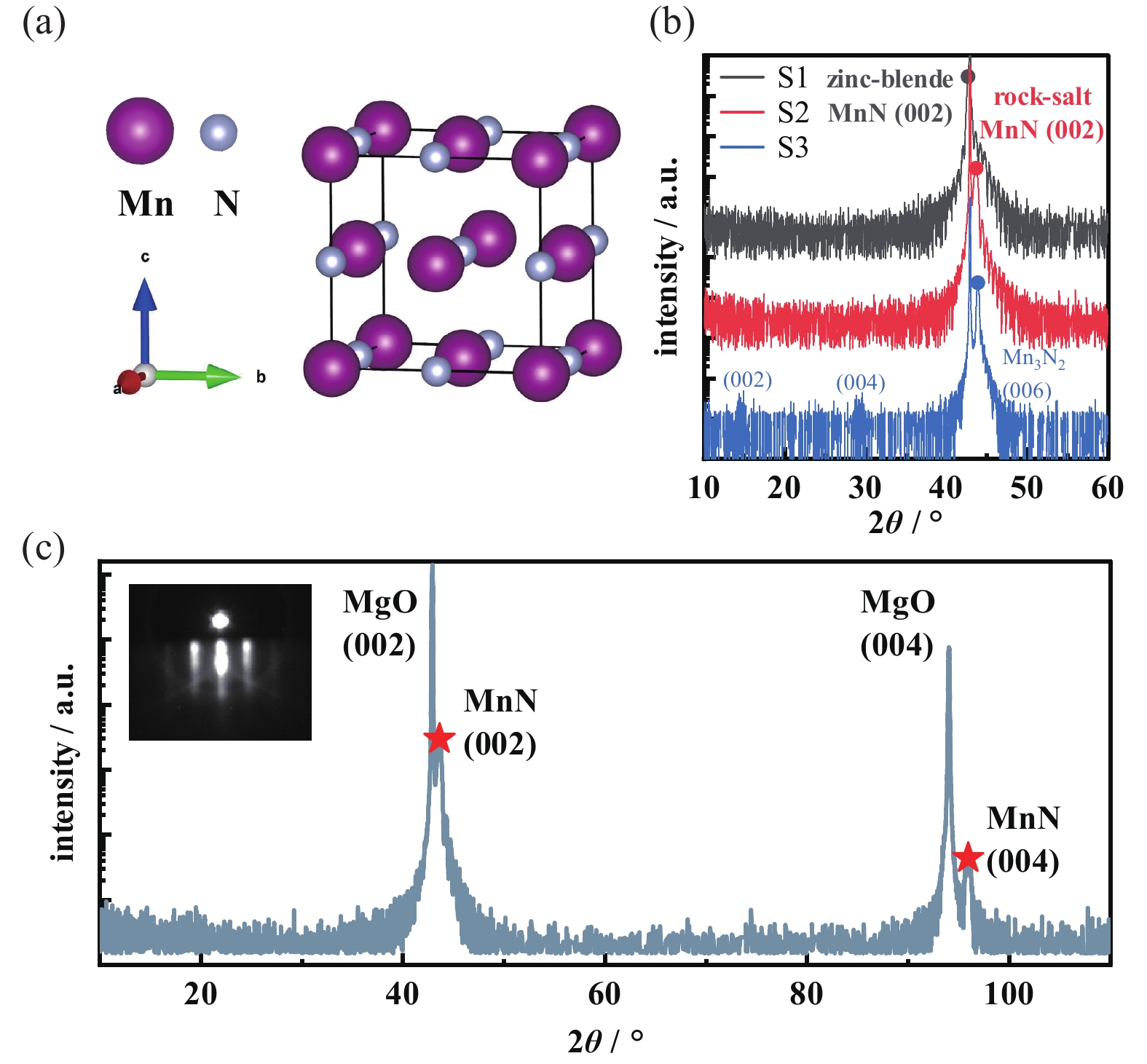
图 1 氮化锰晶格结构的示意图以及最佳生长条件的确认。(a)MnN元胞的示意图,其中紫色和灰色小球分别表示锰原子和氮原子,(b)表一中不同生长条件下样品的XRD谱图,(c)最佳生长条件下所制备MnN的宽范围 θ–2θ XRD谱图。插图是薄膜生长后的RHEED衍射图案
Figure 1. Schematic representation of the MnN crystal structure and identification of optimal growth condition. (a) A schematic diagram of the MnN unit cell, with purple and gray spheres representing Mn and N atoms, respectively, (b) XRD spectra with different growth conditions (summarized in Table 1), (c) Wide-range θ–2θ XRD spectrum of MnN grown under optimal growth conditions. Inset shows RHEED pattern after MnN thin film growth
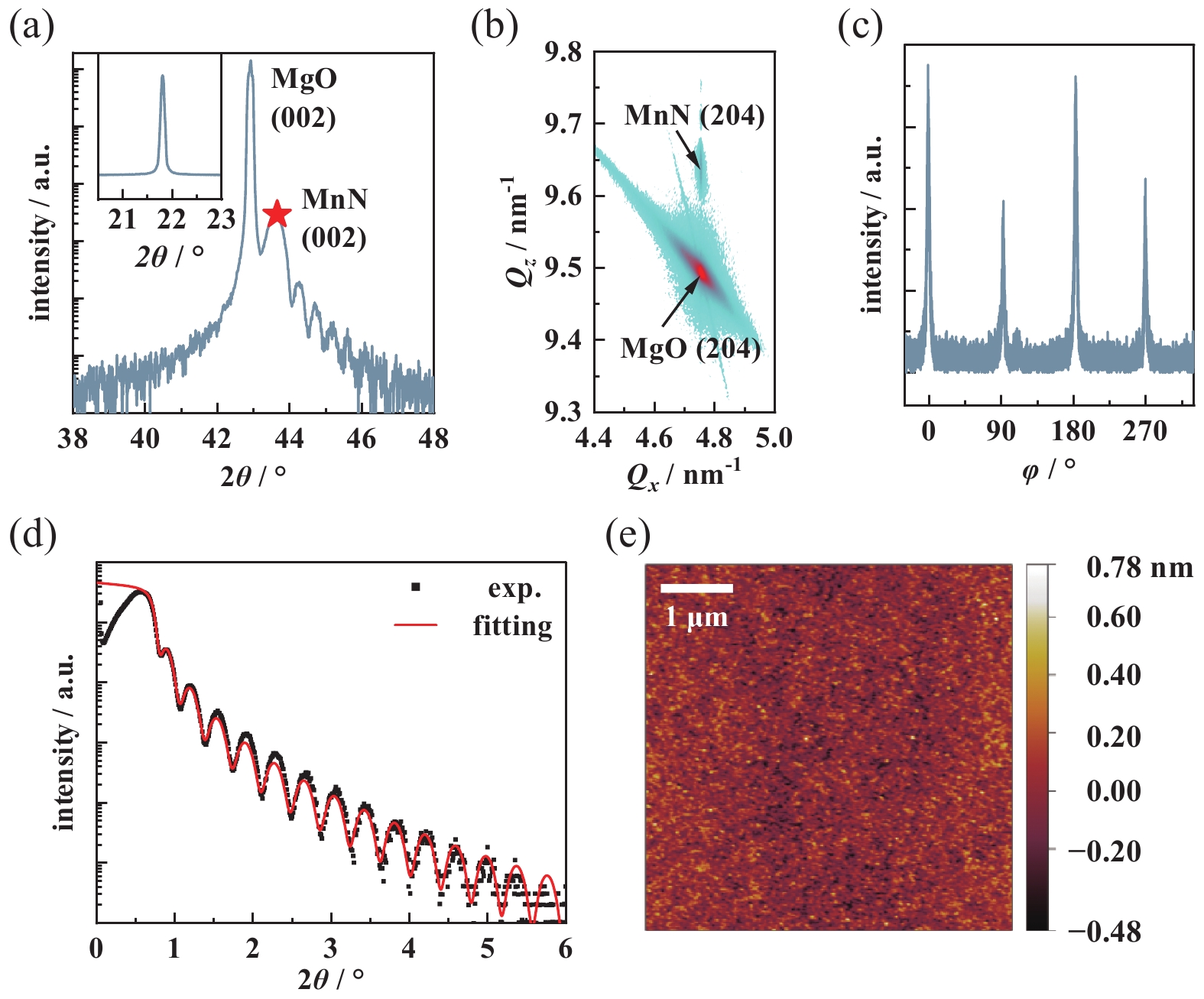
图 2 MgO(001)衬底上23纳米厚MnN薄膜的结构表征。(a)MnN(002)峰附近θ-2θ XRD谱图。插图是(002)峰的摇摆曲线,(b)MgO(204)峰附近的倒易空间成像,(c)MnN(204)峰的360° φ扫描,(d)X射线反射率谱,黑点和红线分别表示实验数据和拟合结果,(e)原子力显微镜得到的薄膜表面形貌图。a.u.为任意单位
Figure 2. Structural characterization of 23-nm-thick MnN grown on MgO (001) substrate. (a) θ-2θ XRD spectrum around the MnN (002) diffraction peak. Inset shows (002) rocking curve, (b) RSM around the MgO (204) reflection, (c) full 360 ° φ-scan around the MnN (204) peaks, (d) X-ray reflectivity (XRR) spectrum, black dots and red line represent the experimental data and fit result, respectively, (e) atomic force microscopy surface morphology characterization. a.u., arbitrary units
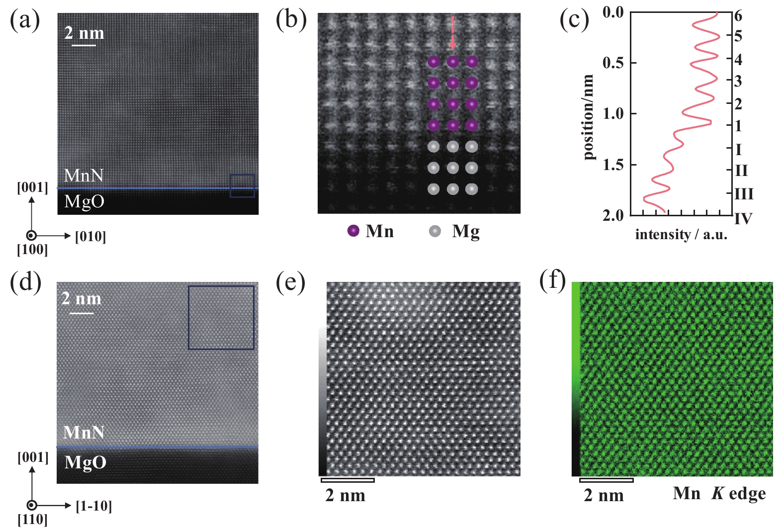
图 3 MnN薄膜的高角度环形暗场扫描透射电镜成像及能量色散能谱表征。(a)沿MgO衬底[100]带轴方向拍摄的MnN薄膜的HAADF-STEM图像,图中蓝色线段标记MnN/MgO界面,(b)图(a)中蓝框区域的局部放大图像,(c)沿(b)图橙色箭头标记区域划线的强度分布曲线,(d)沿MgO衬底[110]带轴方向拍摄的MnN薄膜HAADF-STEM图像,图中蓝色线段标记MnN/MgO界面,(e)图(d)中蓝框区域的局部放大图像,(f)对图(e)区域进行的Mn K-edge EDS元素分布分析图
Figure 3. HAADF-STEM and EDS characterization of the MnN film. (a) HAADF-STEM image of the MnN film taken along the [100] zone axes of MgO, with a blue line indicating the MnN/MgO interface, (b) zoomed-in view of the blue-framed area highlighted in (a), (c) line profile of the intensity across the region marked by orange arrow in (b), (d) HAADF-STEM image of the MnN film taken along the [110] zone axes of MgO, with a blue line indicating the MnN/MgO interface, (e) zoomed-in view of the blue-framed area highlighted in (d), (f) EDS mapping of the Mn K-edge spectrum for the region shown in (e)
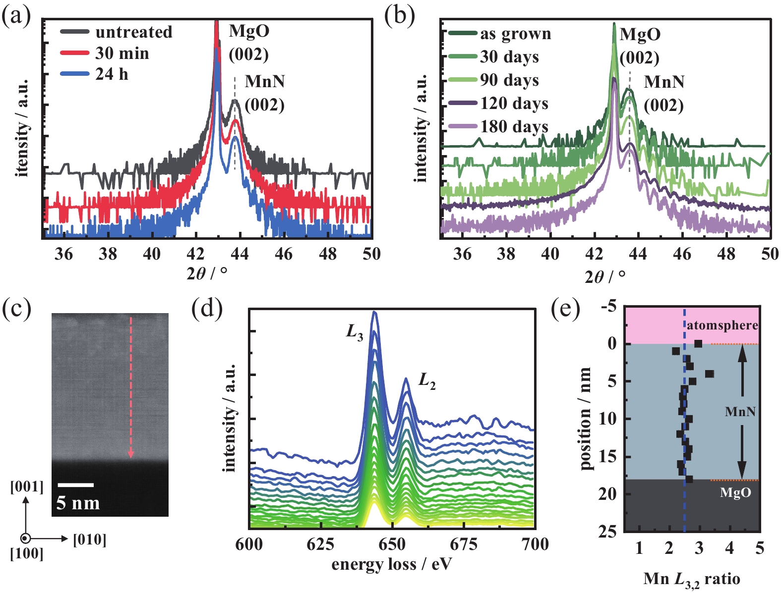
图 4 不同环境条件下MnN薄膜的稳定性表征。(a)不同水浸泡时间下MnN薄膜(002)峰附近的小范围θ-2θ XRD谱图,(b)薄膜制备后不同存放时间下MnN薄膜(002)峰附近小范围θ-2θ XRD谱图,(c)沿MgO衬底[100]带轴拍摄的MnN薄膜HAADF-STEM图像,(d)沿(c)图橙色标记区域的EELS分析,(e)Mn L3/L2带边的积分强度比值
Figure 4. Stability characterization of MnN film under different environmental conditions. (a) Short-range θ-2θ XRD spectra around the (002) diffraction peak of the MnN film at different times in water, (b) Short-range θ-2θ XRD spectra around the (002) diffraction peak of the MnN film at different times after film preparation, (c) HAADF-STEM image of MnN film taken along the [100] zone axes of the MgO substrate, (d) EELS analysis across the orange-marked region in (c), (e) Intensity ratio of Mn L3 to L2 band edge
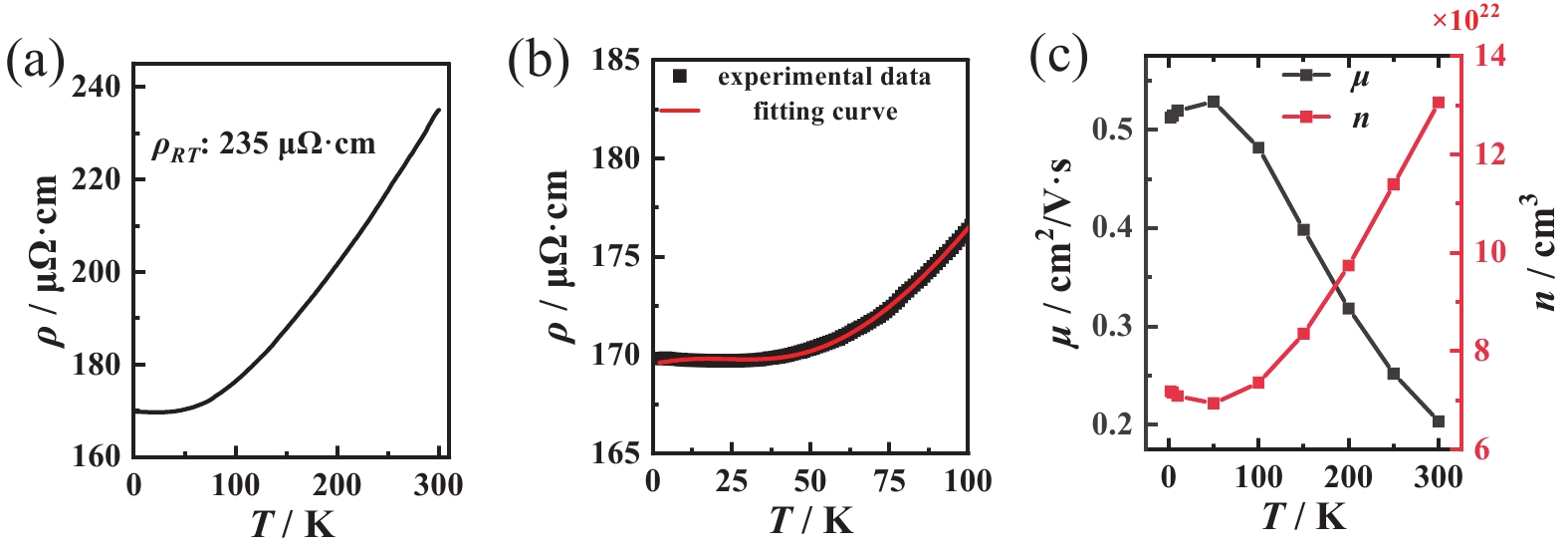
图 5 电输运特性。(a)电阻率−温度曲线,室温(300 K)电阻率值为235 μΩ·cm,(b)2−100开尔文温度区间内实验电阻率数据(黑点)和近藤效应模型的拟合结果(红线),(c)基于电输运测量得到的载流子浓度(n)和迁移率(μ)随温度的变化
Figure 5. Electrical transport properties. (a) Resistivity-temperature curve, with a room-temperature (300 K) resistivity of 235 μΩ·cm, (b) Experimental resistivity measurements (black dots) from 2 K to 100 K and fitting curves derived from the Kondo effect model (red line), (c) Temperature-dependent evolution of carrier concentration (n) and mobility (μ) derived from electrical transport measurements
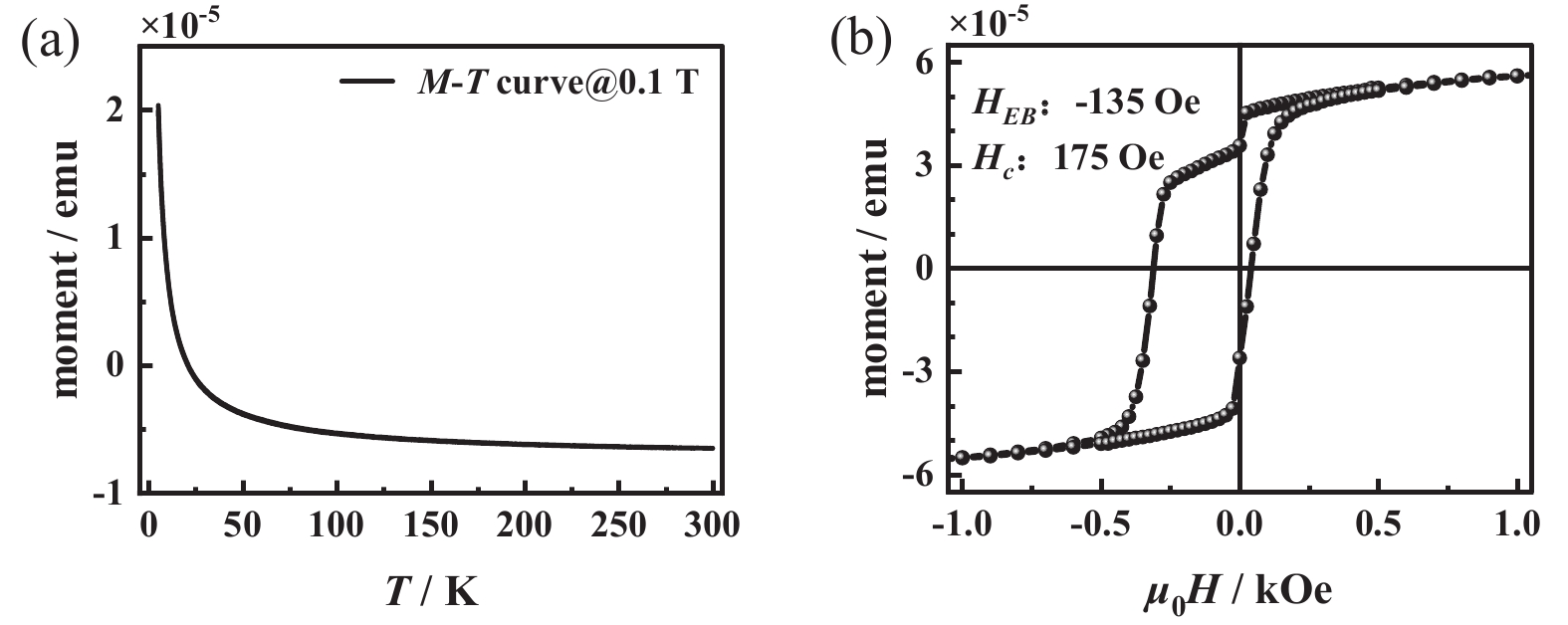
图 6 磁性表征。(a)在1000奥斯特磁场场冷下的MnN薄膜磁化强度−温度曲线,(b)室温(300 K)下MnN/CoFeB的磁滞回线表征
Figure 6. Magnetic characterization. (a) Magnetization-temperature curve of MnN film under 1 kOe field cooling, (b) room-temperature (300 K) hysteresis loop characterization of MnN/CoFeB heterostructure
表 1 图1中3个样品的生长条件和结晶相
Table 1. Growth conditions and resulted crystalline phases of three samples shown in Fig.1
Growth condition Crystalline phase Tsub /℃ TMn /℃ pN /(mbar) S1 300 750 6×10⁻⁵ zinc-blende MnN S2 300 750 3×10⁻⁵ rock-salt MnN S3 300 750 1×10⁻⁵ Mn3N2  下载: 导出CSV
-
[1] Baltz V, Manchon A, Tsoi M, et al. Antiferromagnetic spintronics[J]. Reviews of Modern Physics, 2018, 90(1): 015005 doi: 10.1103/RevModPhys.90.015005 [2] Jungwirth T, Marti X, Wadley P, et al. Antiferromagnetic spintronics[J]. Nature Nanotechnology, 2016, 11(3): 231−241 doi: 10.1038/nnano.2016.18 [3] Olejník K, Seifert T, Kašpar Z, et al. Terahertz electrical writing speed in an antiferromagnetic memory[J]. Science Advances, 2018, 4(3): eaar3566 doi: 10.1126/sciadv.aar3566 [4] Xiong D R, Jiang Y H, Shi K W, et al. Antiferromagnetic spintronics: An overview and outlook[J]. Fundamental Research, 2022, 2(4): 522−534 doi: 10.1016/j.fmre.2022.03.016 [5] Lin P H, Yang B Y, Tsai M H, et al. Manipulating exchange bias by spin–orbit torque[J]. Nature Materials, 2019, 18(4): 335−341 doi: 10.1038/s41563-019-0289-4 [6] Peng S Z, Zhu D Q, Li W X, et al. Exchange bias switching in an antiferromagnet/ferromagnet bilayer driven by spin–orbit torque[J]. Nature Electronics, 2020, 3(12): 757−764 doi: 10.1038/s41928-020-00504-6 [7] Qi J, Zhao Y C, Zhang Y, et al. Full electrical manipulation of perpendicular exchange bias in ultrathin antiferromagnetic film with epitaxial strain[J]. Nature Communications, 2024, 15(1): 4734 doi: 10.1038/s41467-024-49214-z [8] Zhu D Q, Guo Z X, Du A, et al. First demonstration of three terminal MRAM devices with immunity to magnetic fields and 10 ns field free switching by electrical manipulation of exchange bias[C]//2021 IEEE International Electron Devices Meeting (IEDM), San Francisco: IEEE, 2021: 17.5. 1−17.5. 4 [9] Nozières J P, Jaren S, Zhang Y B, et al. Blocking temperature distribution and long-term stability of spin-valve structures with Mn-based antiferromagnets[J]. Journal of Applied Physics, 2000, 87(8): 3920−3925 doi: 10.1063/1.372435 [10] Fernandez-Outon L E, O'Grady K, Oh S, et al. Large exchange bias IrMn/CoFe for magnetic tunnel junctions[J]. IEEE Transactions on Magnetics, 2008, 44(11): 2824−2827 doi: 10.1109/TMAG.2008.2001495 [11] Gokcen N A. The Mn-N (Manganese-Nitrogen) system[J]. Bulletin of Alloy Phase Diagrams, 1990, 11(1): 33−42 doi: 10.1007/BF02841582 [12] Yu R, Chong X Y, Jiang Y H, et al. The stability, electronic structure, elastic and metallic properties of manganese nitrides[J]. RSC Advances, 2015, 5(2): 1620−1627 doi: 10.1039/C4RA10914G [13] Yang H Q, Al-Brithen H, Trifan E, et al. Crystalline phase and orientation control of manganese nitride grown on MgO(001) by molecular beam epitaxy[J]. Journal of Applied Physics, 2002, 91(3): 1053−1059 doi: 10.1063/1.1425435 [14] Suzuki K, Kaneko T, Yoshida H, et al. Crystal structure and magnetic properties of the compound MnN[J]. Journal of Alloys and Compounds, 2000, 306(1-2): 66−71 doi: 10.1016/S0925-8388(00)00794-5 [15] Leineweber A, Niewa R, Jacobs H, et al. The manganese nitrides η-Mn3N2 and θ-Mn6N5+x: Nuclear and magnetic structures[J]. Journal of Materials Chemistry, 2000, 10(12): 2827−2834 doi: 10.1039/b006969h [16] Suzuki K, Yamaguchi Y, Kaneko T, et al. Neutron diffraction studies of the compounds MnN and FeN[J]. Journal of the Physical Society of Japan, 2001, 70(4): 1084−1089 doi: 10.1143/JPSJ.70.1084 [17] Tabuchi M, Takahashi M, Kanamaru F. Relation between the magnetic transition temperature and magnetic moment for manganese nitrides MnNγ (0 < γ < 1)[J]. Journal of Alloys and Compounds, 1994, 210(1-2): 143−148 doi: 10.1016/0925-8388(94)90129-5 [18] Vallejo-Fernandez G, Meinert M. Recent developments on MnN for spintronic applications[J]. Magnetochemistry, 2021, 7(8): 116 doi: 10.3390/magnetochemistry7080116 [19] Meinert M, Büker B, Graulich D, et al. Large exchange bias in polycrystalline MnN/CoFe bilayers at room temperature[J]. Physical Review B, 2015, 92(14): 144408 doi: 10.1103/PhysRevB.92.144408 [20] Zilske P, Graulich D, Dunz M, et al. Giant perpendicular exchange bias with antiferromagnetic MnN[J]. Applied Physics Letters, 2017, 110(19): 192402 doi: 10.1063/1.4983089 [21] Chang H W, Chien Y H, Yuan F T, et al. Correlation between phase composition and exchange bias in CoFe/MnN and MnN/CoFe polycrystalline films[J]. AIP Advances, 2020, 10(2): 025035 doi: 10.1063/1.5129820 [22] Quarterman P, Hallsteinsen I, Dunz M, et al. Effects of field annealing on MnN/CoFeB exchange bias systems[J]. Physical Review Materials, 2019, 3(6): 064413 doi: 10.1103/PhysRevMaterials.3.064413 [23] Dunz M, Schmalhorst J, Meinert M. Enhanced exchange bias in MnN/CoFe bilayers after high-temperature annealing[J]. AIP Advances, 2018, 8(5): 056304 doi: 10.1063/1.5006551 [24] Dunz M, Büker B, Meinert M. Improved thermal stability in doped MnN/CoFe exchange bias systems[J]. Journal of Applied Physics, 2018, 124(20): 203902 doi: 10.1063/1.5051584 [25] Dunz M, Meinert M. Role of the Ta buffer layer in Ta/MnN/CoFeB stacks for maximizing exchange bias[J]. Journal of Applied Physics, 2020, 128(15): 153902 doi: 10.1063/5.0021226 [26] Sinclair J, Hirohata A, Vallejo-Fernandez G, et al. Thermal stability of exchange bias systems based on MnN[J]. Journal of Magnetism and Magnetic Materials, 2019, 476: 278−283 doi: 10.1016/j.jmmm.2018.12.018 [27] Rai A, Dunz M, Sapkota A, et al. Unidirectional and uniaxial anisotropies in the MnN/CoFeB exchange bias system[J]. Journal of Magnetism and Magnetic Materials, 2019, 485: 374−380 doi: 10.1016/j.jmmm.2019.04.043 [28] Dunz M, Matalla-Wagner T, Meinert M. Spin-orbit torque induced electrical switching of antiferromagnetic MnN[J]. Physical Review Research, 2020, 2(1): 013347 doi: 10.1103/PhysRevResearch.2.013347 [29] Miao M S, Lambrecht W R L. Structure and magnetic properties of MnN, CrN, and VN under volume expansion[J]. Physical Review B, 2005, 71(21): 214405 doi: 10.1103/PhysRevB.71.214405 [30] Miao M S, Lambrecht W R L. Effects of vacancies and impurities on the relative stability of rocksalt and zincblende structures for MnN[J]. Physical Review B, 2007, 76(19): 195209 doi: 10.1103/PhysRevB.76.195209 [31] Kalescky R, Kraka E, Cremer D. Identification of the strongest bonds in chemistry[J]. The Journal of Physical Chemistry A, 2013, 117(36): 8981−8995 doi: 10.1021/jp406200w [32] Savant C P, Verma A, Nguyen T S, et al. Self-activated epitaxial growth of ScN films from molecular nitrogen at low temperatures[J]. APL Materials, 2024, 12(11): 111108 doi: 10.1063/5.0222995 [33] Ferrante Y, Jeong J, Saha R, et al. Tetragonal Mn3Sn heusler films with large perpendicular magnetic anisotropy deposited on metallic MnN underlayers using amorphous substrates[J]. APL Materials, 2019, 7(3): 031103 doi: 10.1063/1.5066594 [34] Kum H S, Lee H, Kim S, et al. Heterogeneous integration of single-crystalline complex-oxide membranes[J]. Nature, 2020, 578(7793): 75−81 doi: 10.1038/s41586-020-1939-z [35] Lu D, Baek D J, Hong S S, et al. Synthesis of freestanding single-crystal perovskite films and heterostructures by etching of sacrificial water-soluble layers[J]. Nature Materials, 2016, 15(12): 1255−1260 doi: 10.1038/nmat4749 [36] Ji Z R, Hu M K, Xin H L. Mnedgenet for accurate decomposition of mixed oxidation states for Mn XAS and EELS L2, 3 edges without reference and calibration[J]. Scientific Reports, 2023, 13(1): 14132 doi: 10.1038/s41598-023-40616-5 [37] Loomer D B, Al T A, Weaver L, et al. Manganese valence imaging in Mn minerals at the nanoscale using STEM-EELS[J]. American Mineralogist, 2007, 92(1): 72−79 doi: 10.2138/am.2007.2252 [38] Tan H Y, Verbeeck J, Abakumov A, et al. Oxidation state and chemical shift investigation in transition metal oxides by EELS[J]. Ultramicroscopy, 2012, 116: 24−33 doi: 10.1016/j.ultramic.2012.03.002 [39] Wang Z L, Yin J S, Jiang Y D. EELS analysis of cation valence states and oxygen vacancies in magnetic oxides[J]. Micron, 2000, 31(5): 571−580 doi: 10.1016/S0968-4328(99)00139-0 [40] Sahu B R, Kleinman L. Theoretical study of electronic and magnetic properties of MnN[J]. Physical Review B, 2003, 68(11): 113101 doi: 10.1103/PhysRevB.68.113101 [41] Lefakis H, Huang T C, Alexopoulos P. Surface-oxidation-induced phase separation in FeMn thin films[J]. Journal of Applied Physics, 1988, 64(10): 5667−5669 doi: 10.1063/1.342268 [42] Frost W, Alsaud F, Lawrence R A, et al. Towards MnN as a replacement for IrMn[J]. Scientific Reports, 2024, 14(1): 21944 doi: 10.1038/s41598-024-72886-y [43] Vaz F, Rebouta L, Andritschky M, et al. Oxidation resistance of (Ti, Al, Si)N coatings in air[J]. Surface and Coatings Technology, 1998, 98(1-3): 912−917 doi: 10.1016/S0257-8972(97)00127-8 [44] Banakh O, Schmid P E, Sanjinés R, et al. High-temperature oxidation resistance of Cr1−xAlxN thin films deposited by reactive magnetron sputtering[J]. Surface and Coatings Technology, 2003, 163-164: 57−61 [45] Chen H Y, Lu F H. Oxidation behavior of titanium nitride films[J]. Journal of Vacuum Science & Technology A, 2005, 23(4): 1006−1009 [46] Vallejo K D, Cresswell Z, Messecar A S, et al. Synthesis and physical properties of manganese chromium nitride thin films grown via molecular beam epitaxy[J]. The Journal of Physical Chemistry C, 2025, 129(10): 5237−5244 doi: 10.1021/acs.jpcc.4c08738 [47] Yang F, Wang Z Z, Liu Y H, et al. Engineered kondo screening and nonzero berry phase in SrTiO3/LaTiO3/SrTiO3 heterostructures[J]. Physical Review B, 2022, 106(16): 165421 doi: 10.1103/PhysRevB.106.165421 [48] Radu F, Zabel H. Exchange bias effect of ferro-/antiferromagnetic heterostructures[M]//Zabel H, Bader S D. Magnetic heterostructures: advances and perspectives in spinstructures and spintransport. Berlin: Springer, 2008: 97−184 [49] Nogués J, Schuller I K. Exchange bias[J]. Journal of Magnetism and Magnetic Materials, 1999, 192(2): 203−232 doi: 10.1016/S0304-8853(98)00266-2 [50] Singh H, Gupta M, Prakash H, et al. Role of spin-glass-like interfaces in exchange-biased MnN/Fe thin films grown on W buffer layers[J]. Applied Physics Letters, 2024, 125(9): 092404 doi: 10.1063/5.0220165 [51] Sheng P, Zhao Z Y, Benally O J, et al. Thermal contribution in the electrical switching experiments with heavy metal/antiferromagnet structures[J]. Journal of Applied Physics, 2022, 132(7): 073902 doi: 10.1063/5.0098631 -
计量
- 文章访问数: 59
- HTML全文浏览数: 59
- PDF下载数: 0
- 施引文献: 0